


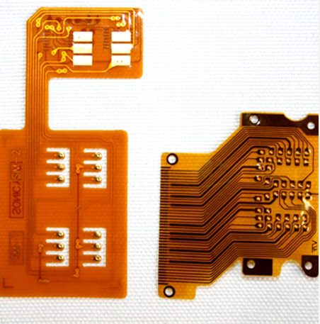
Flexible PCB is a unique type of printed circuit board that replaces the rigid FR4/metal/PTFE/ceramic substrate with a thin, bendable polyimide (PI) substrate and replaces the solder mask with a PI coverlay. Plated through holes or buried vias insulate and protect the conductive copper traces that connect the various flexible PCB layers to the non-conductive PI material. Flexible circuit board, flexible PCB or FPC is another name for flexible PCB.
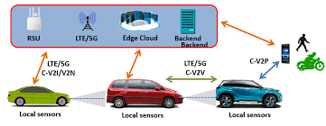
China, as the world’s largest automotive market, has positioned itself as a formidable force in the field of autonomous driving technology. With over 160 OEM manufacturers and a rapidly growing electric vehicle (EV) sector, the nation’s drive toward intelligent mobility is accelerating. This blog explores the current state of autonomous driving technology in China, highlighting key players, technological advancements, and the unique strengths that position China as a global leader in this field.
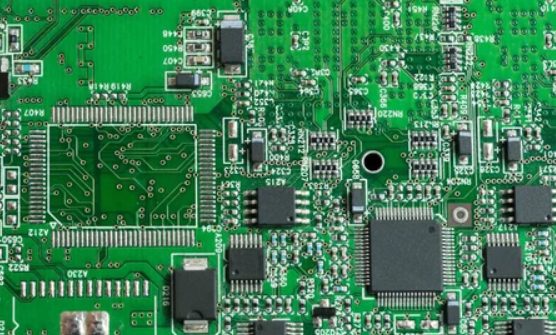
In the fast-paced world of technology, printed circuit boards (PCBs) quietly protect the functionality of electronic devices. In addition to connecting components, PCB assembly is also critical to protecting against potential threats.
BGA is a surface mount component that is used for chip design ICs. The full name of BGA is ball grid array. Therefore, it has many balls in the form of an array. Generally, BGA is used for chip design PCBs such as microprocessors and integrated ICs
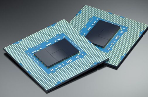
BGA assembly refers to the process of attaching a ball grid array (BGA) to a circuit board using a solder reflow process. BGAs are surface mount components that use an array of solder balls to create electrical interconnections between components and PCBs
When it comes to assembling Printed Circuit Boards (PCBs), there are two primary technologies: Surface Mount Technology (SMT) assembly and Through-Hole Technology (PTH) assembly
Printed circuit board (PCB) assembly is at the heart of electronic components and gadgets. Designers typically choose between two primary techniques for mounting components on PCBs: SMT (Surface Mount Technology) and PTH (Plated Through Hole).
The introduction of phenolic resin-based laminates in the 1930s improved mechanical stability and insulation. However, the game-changer was the development of glass-reinforced epoxy laminates (FR-4) in 1940, offering superior electrical insulation, moisture resistance, and mechanical durability.
A PCB is a substrate or laminate that supports and connects electronic components to enable various device functionalities. Common substrates include FR4 (flame retardant material), but there are alternatives such as polyimide for flexible designs. PCBs are categorized by layers—single-sided, double-sided, and multi-layer—and by substrate type (rigid, flexible, or rigid-flex combinations)
Surface Mount Technology (SMT) board assembly is a critical and widely used process in modern PCB manufacturing. This process involves placing and soldering electronic components directly onto the surface of PCB pads.