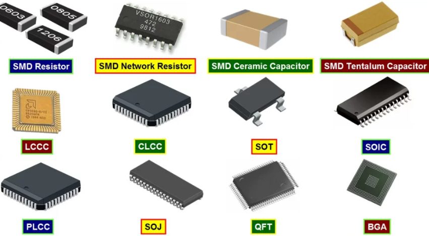
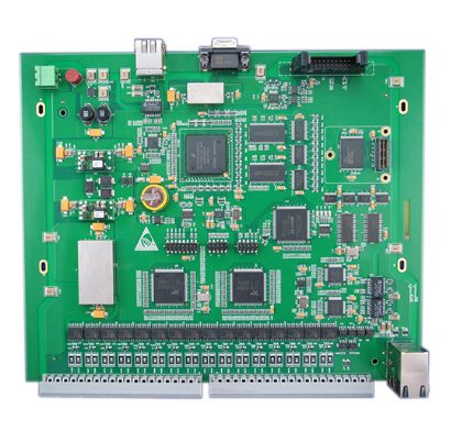
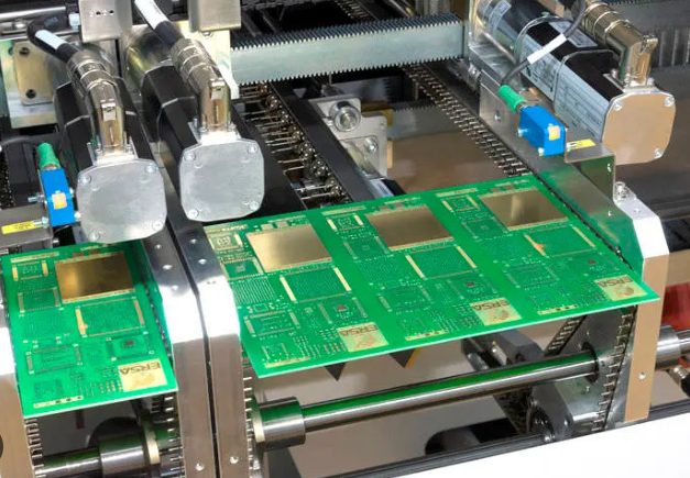
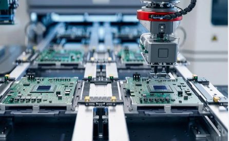
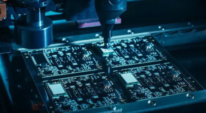
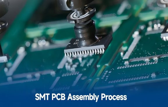
SMD (Surface-Mount Device) components and SMT (Surface-Mount Technology) stickers serve the same electrical functions. However, due to their small size, SMD components offer better electrical performance. Despite these advantages, not all components are available for surface mounting. High-end processors and large connectors like BGAs (Ball Grid Arrays) and PGAs (Pin Grid Arrays) often require mixed assembly modes due to their unique requirements.
Surface Mount Technology (SMT) has revolutionized the electronics industry by enabling compact, efficient, and cost-effective PCB assembly. Today, nearly all commercially manufactured electronic devices utilize SMT for its ability to pack more functionality into smaller spaces and improve manufacturing processes through automation.
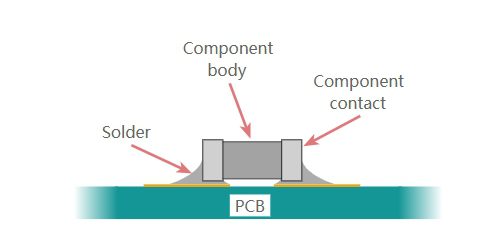
Surface Mount Technology (SMT) is a method of mounting electronic components directly onto the surface of a printed circuit board (PCB). The components used in SMT, called Surface Mount Devices (SMDs), have largely replaced the older through-hole technology in modern electronics manufacturing due to their compact size and compatibility with automated assembly processes.
Have you ever wondered how our gadgets have become so powerful yet so compact? The secret lies in a manufacturing marvel: Surface Mount Technology (SMT) for PCB assembly. In this guide, we’ll break down the essentials of SMT PCB assembly, why it’s the go-to method for modern electronics, and how it’s shaping the tech we rely on today.
Surface Mount Technology (SMT) has transformed electronics manufacturing, becoming the preferred method for assembling printed circuit boards (PCBs). By allowing components to be directly mounted on the PCB surface without requiring wires or leads through holes, SMT offers unparalleled advantages in miniaturization, automation, and reliability. However, like any technology, SMT has its challenges. This guide explores the advantages, challenges, and decision-making factors for SMT PCB assembly to help you determine if it suits your specific needs.
SMT PCB Assembly plays a vital role in the electronics manufacturing industry, enabling the production of compact, complex, and reliable electronic devices. This process combines Surface Mount Technology (SMT) with Printed Circuit Board (PCB) assembly to create functional electronic circuits or modules. Below is a detailed breakdown of the terms, steps, and importance of SMT PCB assembly.
When assembling a printed circuit board (PCB), components are mounted onto the board through one of two primary methods: Surface Mount Technology (SMT) or Through-Hole Technology (THT). Each method has distinct advantages and is suited to different applications depending on the project requirements.
SMT is a process of constructing electronic circuits by placing components directly onto the surface of a PCB. Unlike the earlier through-hole technology, which required drilling holes for component leads, SMT simplifies the manufacturing process while enabling smaller, more intricate designs.
There are three main sources of heat in PCB: heat from electronic components; heat from PCB itself; Heat from other parts.
Among the three heat sources, the heating from electronic components is the largest, followed by the heat generated by PCB board, and other heat from the outside based on the overall thermal design of the system.
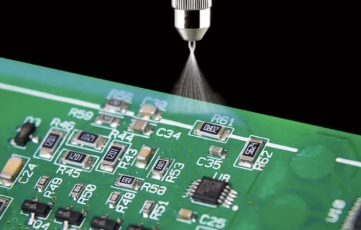
Conformal coatings play a critical role in ensuring the longevity and reliability of printed circuit boards (PCBs). Whether designing electronics for consumer devices, automotive systems, or military applications, selecting the right conformal coating is essential.

