


Project Background A manufacturing plant in California sought to reduce electricity costs through a distributed rooftop solar system while enhancing its green and sustainable corporate image. With ample rooftop space available, the company required a highly efficient MPPT solar controller capable of maximizing solar energy utilization and ensuring stable operation. ⚡The Role of PCBA Technology […]

The customer is a globally leading manufacturer of communication equipment, specializing in the development and production of large-scale routers, switches, servers, and high-speed networking devices. As modern network communications demand increasingly high signal integrity, reliability, and thermal stability, the customer required an 18-layer PCB with low-loss material (S1000-2M) and advanced immersion gold plating to ensure stable signal transmission and long-term reliability
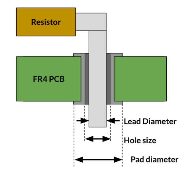
In printed circuit board (PCB) design, copper pads are points for attaching components with soldering. These pads come in two primary types: through-hole and surface-mount (SMD). Through-hole pads are designed for components with leads that are inserted through the pad’s holes and soldered on the opposite side of the board. This method ensures a mechanical and electrical bond between the component and the PCB, beneficial for long-term reliability. Read on as we discuss through-hole pad design.
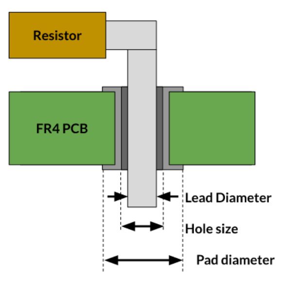
In printed circuit board (PCB) design, the choice of pad type plays a critical role in determining the durability, reliability, and performance of the final product. Through-hole pads, which are designed for components with leads that pass through the PCB, offer superior mechanical and electrical connections compared to surface mount pads.
Low power circuit design includes strategies focused on minimizing both dynamic and static power usage in your printed circuit boards. While selecting components with low power requirements is a crucial element, low power PCB design involves more comprehensive considerations to effectively manage power consumption.
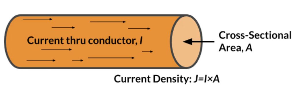
Copper current density refers to the amount of continuous current going through a copper wire —whether on a circuit board as a trace or not. According to the principles of Joule or Ohmic heating (represented as VI or I²R), any material that conducts electricity will generate heat, leading to a gradual rise in temperature in both the conductor and its surrounding environment.
The primary challenge of this project was ensuring that the high-frequency PCB maintained extremely low attenuation and distortion during signal transmission while preventing external interference from affecting signal quality.
kups is one of the most critical aspects of HDI PCB design. Vias in HDI PCBs offer greater flexibility compared to standard boards, but they also significantly impact manufacturing costs and reliability.
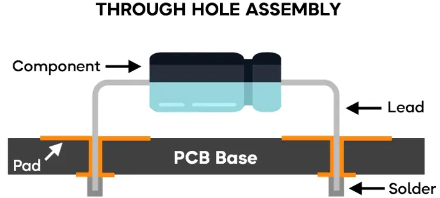
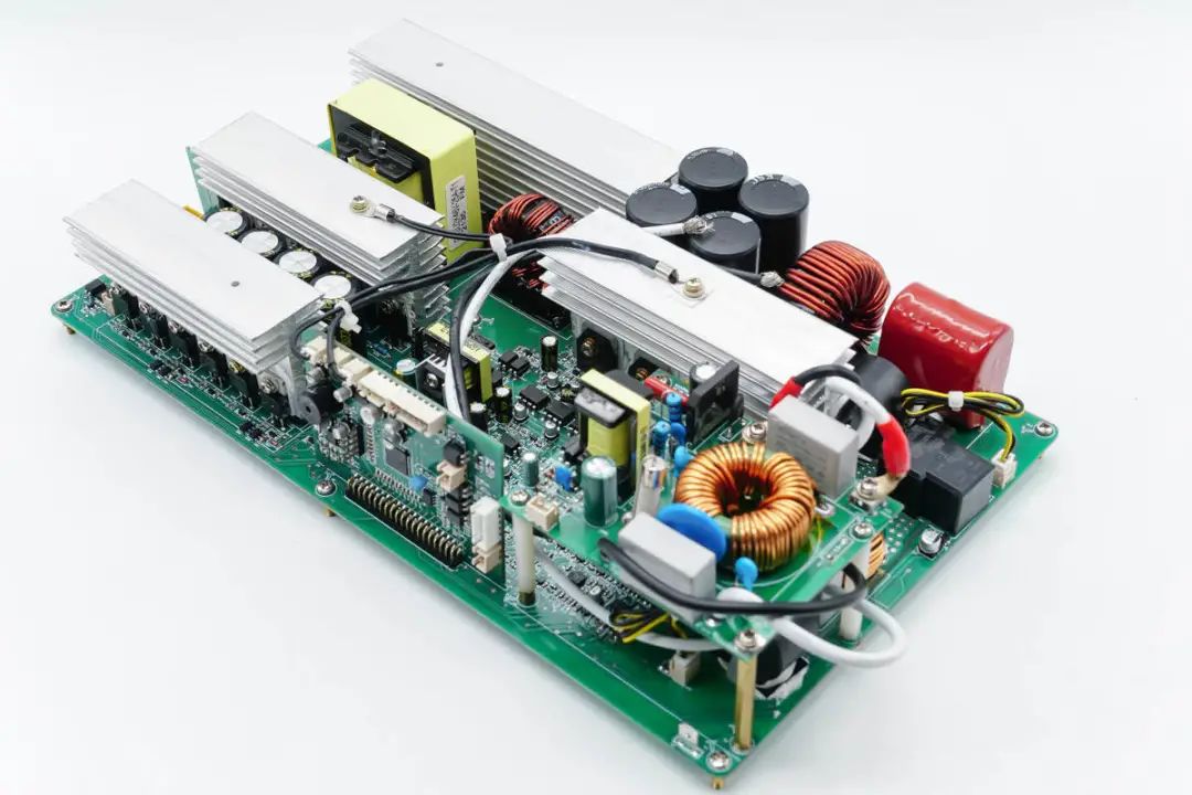
One of the two most common methods of attaching electronic components to PCBs is the through-hole or through-hole process. This technology is older than SMT, and for many years, it was the standard technology for PCB assembly. When surface mount technology became popular in the 1980s, many people thought it would make through-hole PCB assembly obsolete. However, through-hole technology has several advantages that make it still a preferred choice for certain applications.
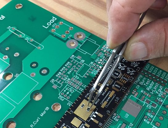
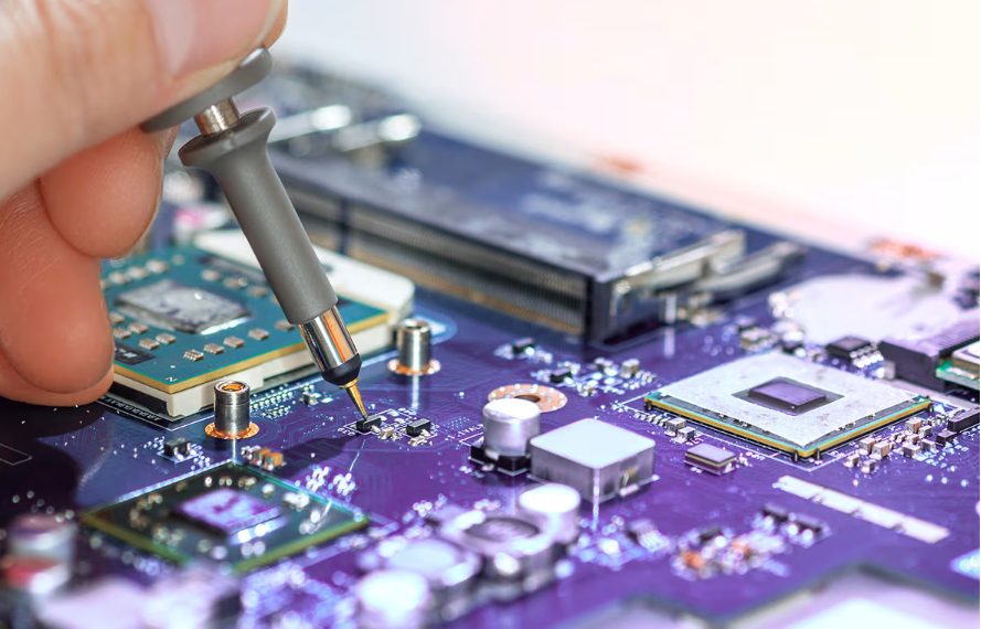
Basic soldering guide on how to solder electronic components to a printed circuit board (PCB). This is a detailed and complete soldering guide for both automated soldering in mass production and manual soldering in PCB rework and repair.