


1. Background Overview With the growing demand for smart cities and industrial automation, air quality monitoring systems have become critical in factories, laboratories, smart buildings, and underground facilities. A European client developing a gas sensor module for air quality detection required a high-precision, low-power, and stable PCBA solution with strong anti-interference capability. KKPCB was selected […]
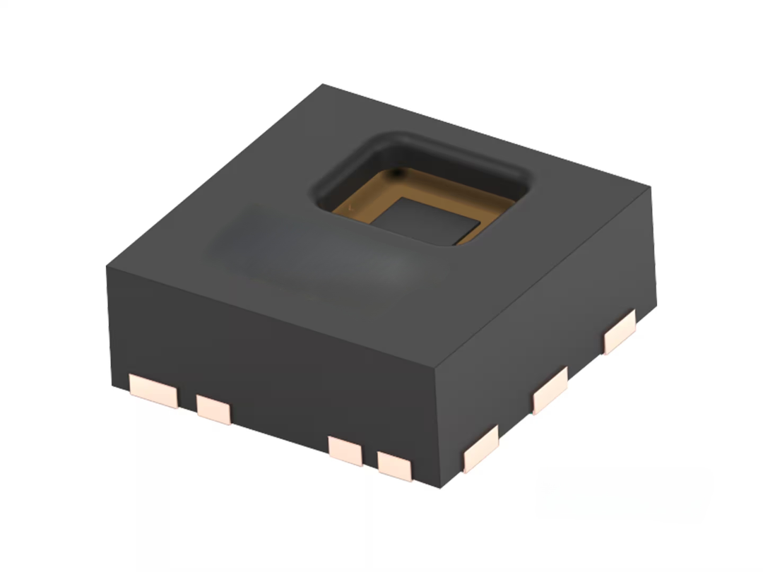
1. Background Overview A European client in the industrial automation sector required a compact, highly accurate humidity and temperature sensor solution with stable performance under harsh environmental conditions. To meet this demand, KKPCB was entrusted with providing a reliable, cost-efficient, and fast-delivery PCBA manufacturing solution for this sensor project. 2. Application Scenario The humidity and […]
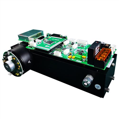
1. Background Overview Under the accelerating global trend of industrial automation, a client from Europe aimed to develop a servo drive product with high dynamic response, high-precision control, and high integration for their next-generation industrial automation equipment. After evaluating multiple suppliers, the client ultimately chose to collaborate with KKPCB, seeking a one-stop customized service from […]
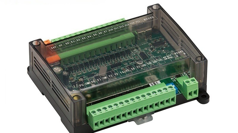
1️⃣ Background Overview With the tightening of global environmental regulations and the upgrading of industrial water resource management needs, sewage treatment plants of customers in Europe, America and the Middle East are in urgent need of highly reliable and extreme environment resistant automation control systems. Traditional PLC modules have pain points such as frequent signal […]
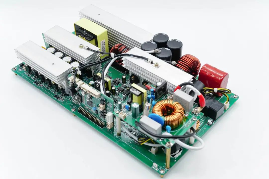
Project Background A manufacturing plant in California sought to reduce electricity costs through a distributed rooftop solar system while enhancing its green and sustainable corporate image. With ample rooftop space available, the company required a highly efficient MPPT solar controller capable of maximizing solar energy utilization and ensuring stable operation. ⚡The Role of PCBA Technology […]

The customer is a globally leading manufacturer of communication equipment, specializing in the development and production of large-scale routers, switches, servers, and high-speed networking devices. As modern network communications demand increasingly high signal integrity, reliability, and thermal stability, the customer required an 18-layer PCB with low-loss material (S1000-2M) and advanced immersion gold plating to ensure stable signal transmission and long-term reliability
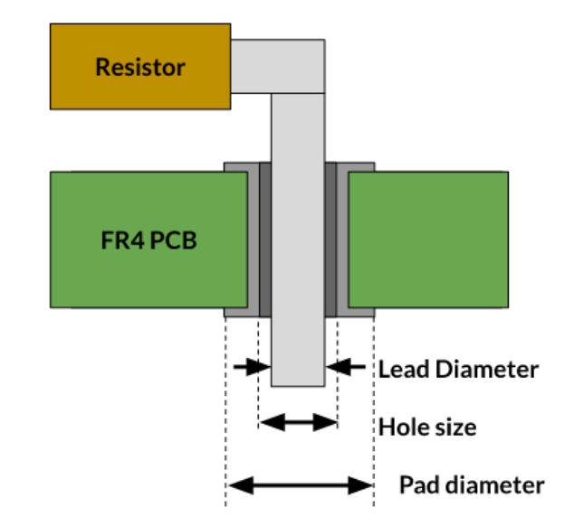
In printed circuit board (PCB) design, copper pads are points for attaching components with soldering. These pads come in two primary types: through-hole and surface-mount (SMD). Through-hole pads are designed for components with leads that are inserted through the pad’s holes and soldered on the opposite side of the board. This method ensures a mechanical and electrical bond between the component and the PCB, beneficial for long-term reliability. Read on as we discuss through-hole pad design.
In printed circuit board (PCB) design, the choice of pad type plays a critical role in determining the durability, reliability, and performance of the final product. Through-hole pads, which are designed for components with leads that pass through the PCB, offer superior mechanical and electrical connections compared to surface mount pads.
Low power circuit design includes strategies focused on minimizing both dynamic and static power usage in your printed circuit boards. While selecting components with low power requirements is a crucial element, low power PCB design involves more comprehensive considerations to effectively manage power consumption.
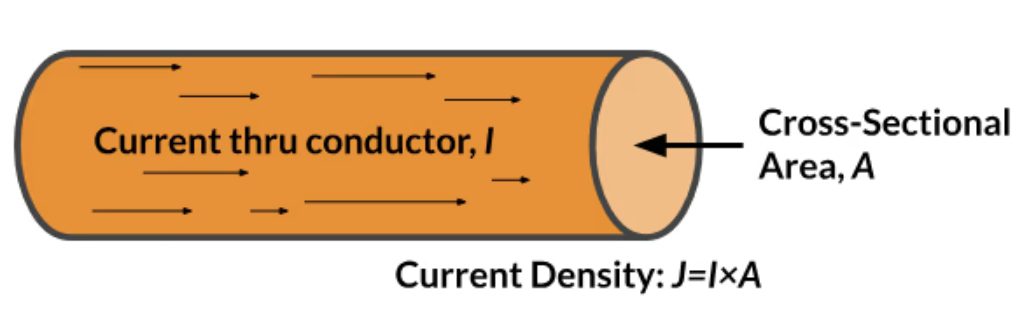
Copper current density refers to the amount of continuous current going through a copper wire —whether on a circuit board as a trace or not. According to the principles of Joule or Ohmic heating (represented as VI or I²R), any material that conducts electricity will generate heat, leading to a gradual rise in temperature in both the conductor and its surrounding environment.