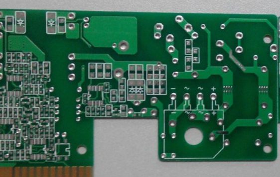
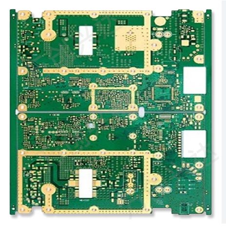
Nano waterproofing agent can be understood as nano waterproof coating, nano moisture-proof coating, anti-salt spray corrosion coating from the function, which provides a better solution for the waterproof of electronic products.The nano coating is directly applied to the PCBA of electronic products by immersion and spraying
Ensuring Electromagnetic Compatibility (EMC) compliance in motor control PCBs is essential to avoid interference issues, maintain system reliability, and ensure regulatory approval for market access.
The output value of the global electroplating PCB industry accounts for the rapid growth of the proportion of the total output value of the electronic component industry. It is the industry with the largest proportion in the electronic component industry. It occupies a unique position
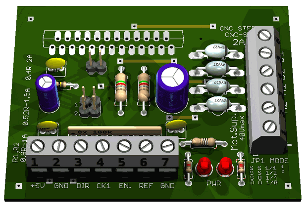
A motor controller is an electronic or electrical device used to regulate the speed, torque, and position of a motor. It can automatically or manually start, stop, and protect the motor from issues like overloads.
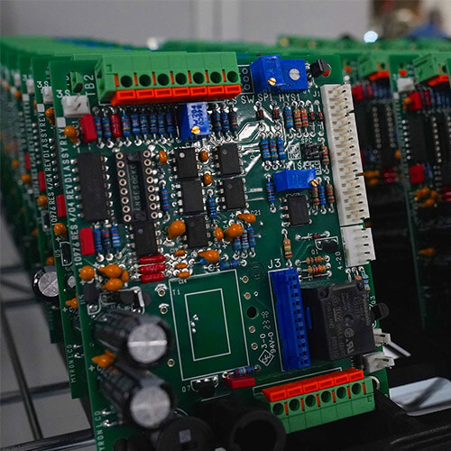
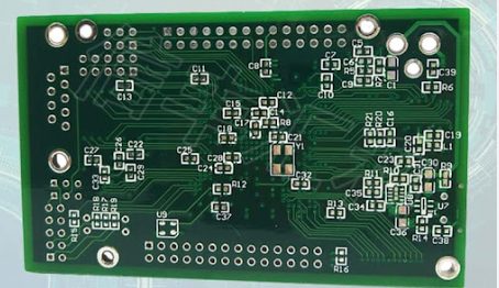
Circuit boards play a key role in making sure electronic products work properly. They provide structural support and link all the electrical parts together. Whether it’s in smartphones, laptops, or household devices, none could operate without a PCB
As an increasing variety of everyday electronic components began to rely on circuit boards, the race was on to develop simpler, more compact alternatives, and this led to the development of the material, PCB. With PCB materials, circuits can be routed between a host of different components. The metal that facilitates the transfer of current between the board and any attached components is known as solder, which also serves a dual purpose with its adhesive qualities
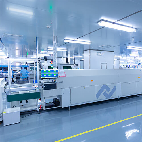
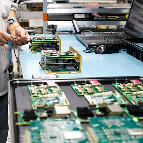
KKPCB provides global customers with one-stop services from PCB layout, prototype PCB proofing, PCB manufacturing, PCBA processing (including SMT and DIP), PCBA testing, PCBA product assembly and outbound packaging. You could provide a Gerber file or BOM list to us, we will offer the finished PCB products or PCB assembly which are satisfied with you
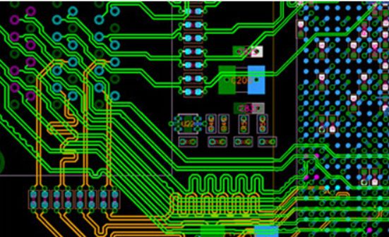
Addressing power supply noise interference in PCB design involves a systematic approach to layout optimization, filtering, and grounding. By understanding the root causes of power supply noise and applying the countermeasures outlined above, designers can significantly enhance circuit performance and reliability. A clean power supply, well-isolated signal paths, and proper filtering are key to achieving a noise-resilient PCB.
Careful adherence to these guidelines ensures efficient and reliable mobile phone PCB designs. By prioritizing critical signal paths, ensuring proper grounding, and optimizing power distribution, potential risks in wiring are mitigated, resulting in better performance and reduced EMI issues.
Incorporating schematic simulation into the PCB design process not only saves valuable time but also increases the accuracy and efficiency of the entire workflow. By automating the process of checking for errors and verifying connections, designers can improve the overall quality of the PCB and minimize the chances of issues in the final design.

