


Low power circuit design includes strategies focused on minimizing both dynamic and static power usage in your printed circuit boards. While selecting components with low power requirements is a crucial element, low power PCB design involves more comprehensive considerations to effectively manage power consumption.

Military and aerospace PCBs must adhere to intensely high standards to ensure their safety and functionality in the extreme conditions they’re used in. For this reason, PCB design for military and aerospace applications requires incredibly stringent guidelines with built in redundancy, extra safety, and stringent tolerances, minimizing risk of failure
When designing a printed circuit board (PCB), engineers often focus on ensuring the correct impedance structures and electrical performance of the board. However, the physical characteristics, such as PCB thickness, are equally important and can significantly impact the cost, manufacturability, and performance of the final product. While standard PCB thicknesses are widely used, they are more of a convention than a strict requirement, offering designers an opportunity for optimization, especially in high-volume production.
A Hybrid Printed Circuit Board (PCB) is a multilayer PCB that combines dissimilar materials to optimize electrical performance, improve system reliability, and enhance high-frequency RF applications.
As we step into 2025, the electronics manufacturing industry is poised for transformative changes driven by technological advancements, shifting consumer demands, and global economic factors. At KKPCB, we are committed to staying at the forefront of these developments to deliver cutting-edge solutions to our clients. Here’s an overview of the key trends set to reshape the industry this year.
Surface finishes in PCBs are vital for ensuring solderability, electrical conductivity, and corrosion resistance. They help components bond securely to the board, ensure smooth signal flow, and protect the PCB from environmental damage. Without a proper surface finish, a PCB may not function correctly or could wear out faster.
Staggered vias are a crucial element in the world of printed circuit board (PCB) design, especially for high-density interconnect (HDI) boards. But what exactly are they? Why are they important? Let’s take a deep dive into staggered vias and their benefits
High frequency PCBs are specialized circuit boards designed to transmit signals over a gigahertz (GHz) frequency range, ensuring quick and reliable communication in devices ranging from military radar systems to smartphones.
With the continuous development of high-frequency electronic devices, especially in wireless networks and satellite communications, information products are becoming faster and higher in frequency, and communication products are moving towards large capacity and high-speed wireless transmission for voice, video, and data standardization. As a result, the next generation of products requires high-frequency substrates. The process technology for high-frequency PCB production is continuously improving to meet the diverse needs of users. Based on over ten years of experience in PCB production, this article will detail the key technical aspects and considerations for the production of high-frequency microwave PCBs.
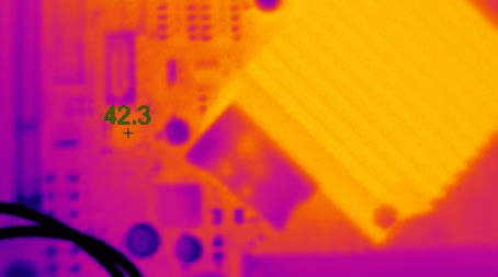
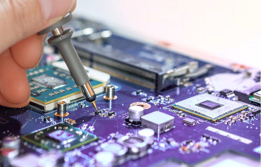
With the continuous development of electronic components, thermal management in modern electronic products has become increasingly important. Especially in highly integrated and miniaturized electronic devices, ensuring that circuit boards and components operate within the proper temperature range is a critical task for enhancing product performance and reliability. Infrared thermal imaging technology, as a non-contact temperature measurement tool, has been widely applied in the design, validation, fault diagnosis, and thermal management processes of electronic products. This article will explore the basic principles, advantages, and applications of infrared thermal imaging in the electronics industry, specifically how it helps optimize thermal management and improve product performance.