


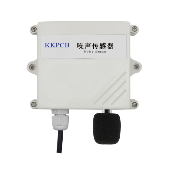
1. Background Overview A European client planned to develop an industrial-grade noise sensor for factory noise monitoring and smart city applications. The PCBA needed to meet strict requirements for sensitivity, interference immunity, and long-term reliability. Challenges included precise signal processing, limited PCB space, environmental adaptability, and cost control. 2. Application Scenarios The noise sensor is […]
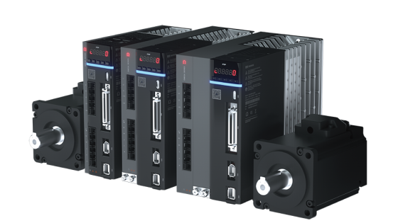
Industry Challenges
Legacy System Limitations: 60% of CNC retrofits require motion control upgrades (ABI Research 2024)
Precision Demands: PCB drilling needs ±5μm positioning accuracy at 120IPM
Cost Pressure: Traditional solutions exceed $3k/axis
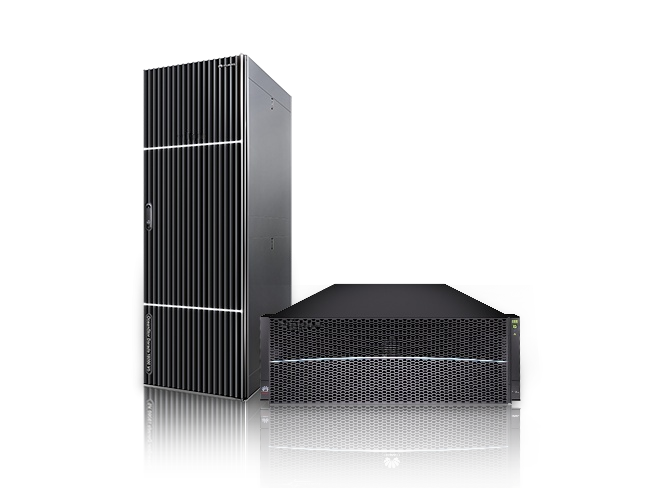
1. Background Overview With the rising demand for data processing and real-time analysis in industrial automation systems, high-speed and reliable data storage devices have become essential. A European industrial equipment manufacturer approached KKPCB for a customized PCBA solution for their new-generation data storage modules. The goal was to ensure high performance, reliability, and cost-efficiency under […]
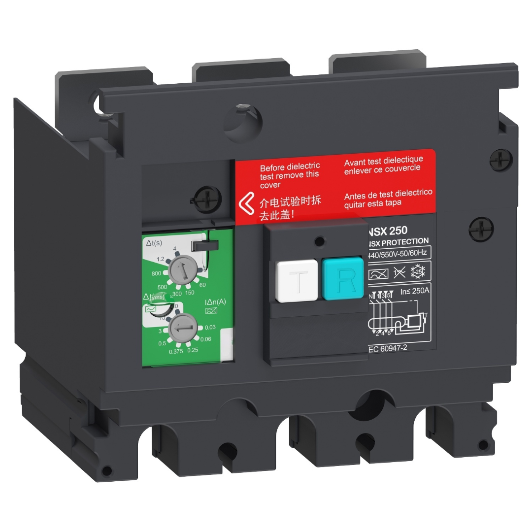
1. Background Overview In the context of Industry 4.0, safety and reliability are paramount in industrial automation systems. A European client developing a leakage protection module sought a PCBA solution that ensures high precision, rapid response, and compliance with international safety standards. KKPCB was selected to provide a customized PCBA solution to meet these stringent […]

Industry Challenges in Thermal Testing
Measurement Complexity: 73% of electronic component failures originate from thermal stress (IEEE Reliability Report)
Channel Limitations: Conventional systems max out at 64 channels with 1.5°C accuracy
Data Integration: 68% testing time wasted on multi-instrument synchronization
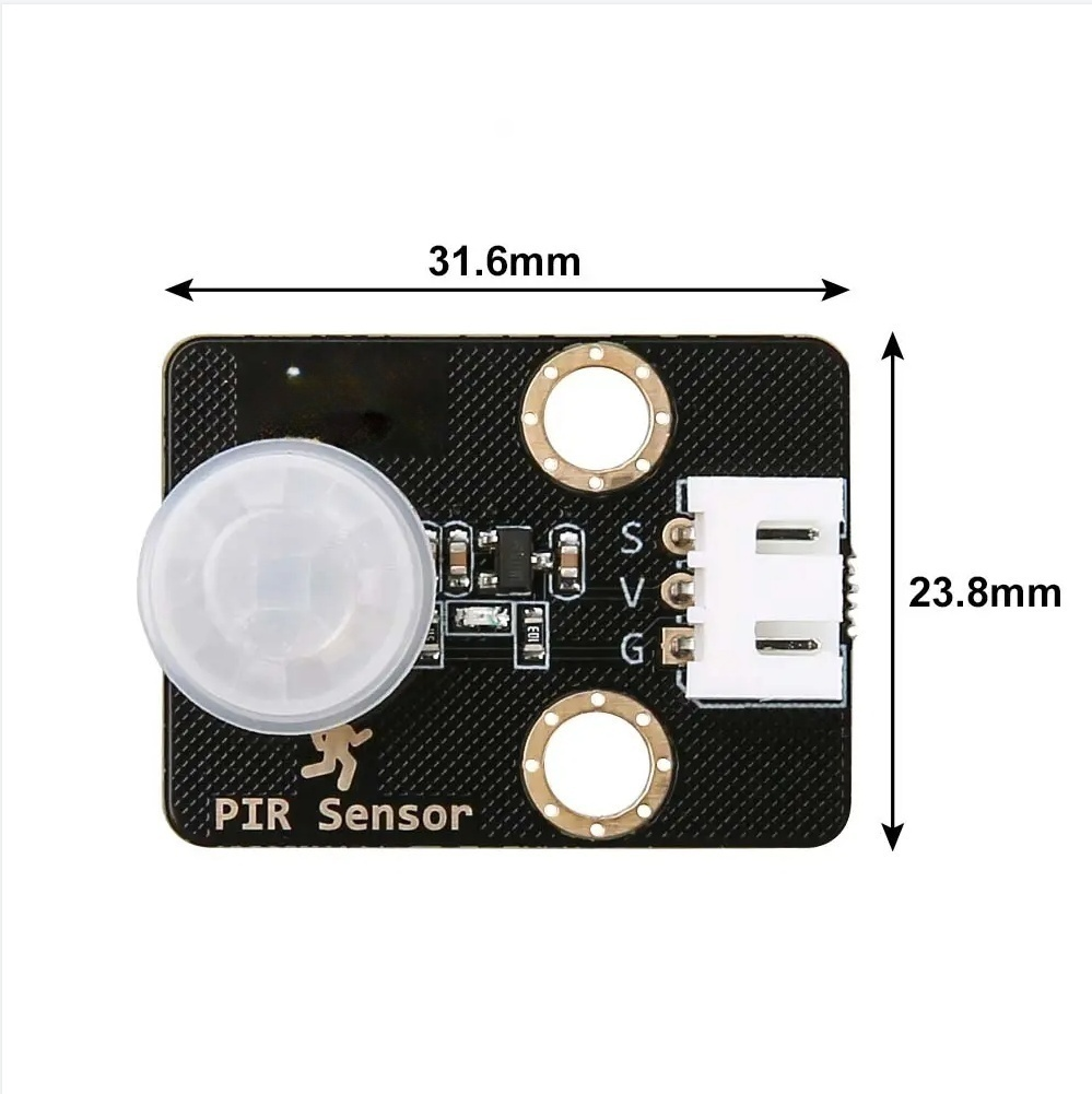
1. Background Overview In industrial automation systems, sensors play a vital role in enabling intelligent monitoring and equipment interaction. A European client recently sought to develop a PIR-based motion sensor module for use in equipment activity detection and control systems. The module required high sensitivity, strong anti-interference capability, low power consumption, and stable performance in […]
1. Background Overview With the growing demand for smart cities and industrial automation, air quality monitoring systems have become critical in factories, laboratories, smart buildings, and underground facilities. A European client developing a gas sensor module for air quality detection required a high-precision, low-power, and stable PCBA solution with strong anti-interference capability. KKPCB was selected […]

1. Background Overview A European client specializing in industrial automation required a compact, highly reliable smart sensor capable of accurately detecting humidity, temperature, and motion in challenging environments. To meet strict industrial requirements—such as signal integrity, durability, and fast time-to-market—they collaborated with KKPCB to develop a tailored PCBA solution. 2. Application Scenario The smart sensor […]
I. Innovation Background
Market Pain Points
Battery Dependency: 78% of wireless doorbell failures caused by battery issues (Consumer Reports 2023)
Installation Limitations: Wired solutions require complex retrofitting
Range Reliability: Typical products fail beyond 30m/2 walls
1. Background Overview A European client in the industrial automation sector required a compact, highly accurate humidity and temperature sensor solution with stable performance under harsh environmental conditions. To meet this demand, KKPCB was entrusted with providing a reliable, cost-efficient, and fast-delivery PCBA manufacturing solution for this sensor project. 2. Application Scenario The humidity and […]