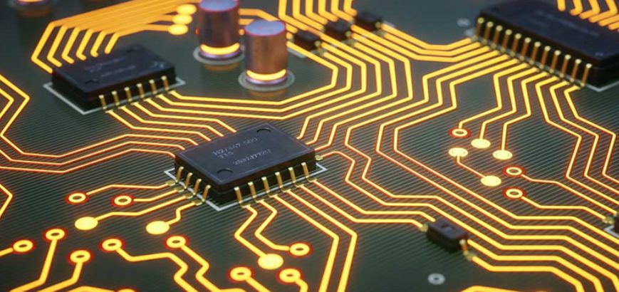
The emergence of humanoid robots, equipped with human-like movement, perception, and intelligence, represents the next frontier of robotics. Central to this development is the advancement of printed circuit boards (PCBs) which enable the intricate control, decision-making, and sensing capabilities of these robots. This blog explores how PCB technology is powering humanoid robots and its implications for the future.
Evolution of Medical PCB Assembly
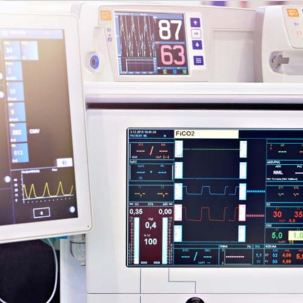
There is more to the advancement of technology and medical devices, and people may no longer need the services of hospitals and doctor’s offices. Medical PCB services are a result of evolution that makes medical operations easier and more stress-free. Diagnosis is one of the key steps to fully utilize these electronic devices to minimize treatment time and increase treatment efficiency.
In recent years, electronic products have become increasingly complex and integrated into people’s daily lives. However, there are still two popular methods for soldering electronic components together to build circuits:
Surface Mount Technology (SMT) for PCB Assembly
Through-Hole (PTH) PCB Assembly
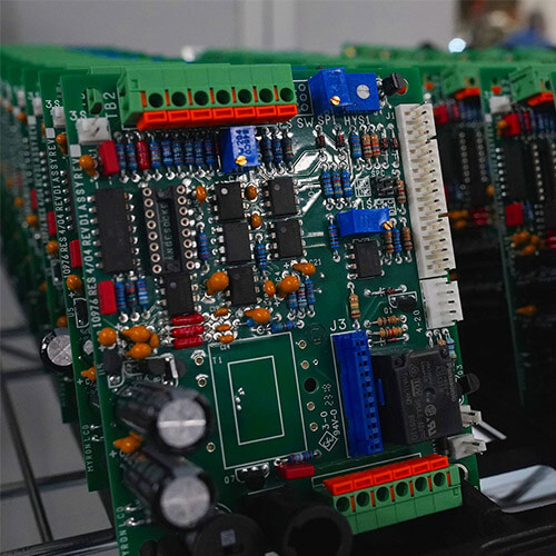
Surface mount SMT PCB assembly is not easy to assemble PCBs using standard components with leads. Resistors and capacitors need pre-formed information, and even the leads of integrated circuits must be adjusted to the exact right pitch so that they can be inserted into the holes.
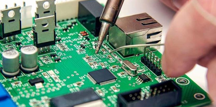
Manufacturers use flux to solder components on PCBs. Depending on the PCB components, flux also varies and is used to fix them on the board. It ensures uninterrupted and strong electrical connections between devices. However, it is crucial to remove excess flux so as not to blur signal traces or damage connections. In this article, we have introduced various methods and basic steps to remove flux from PCBs.
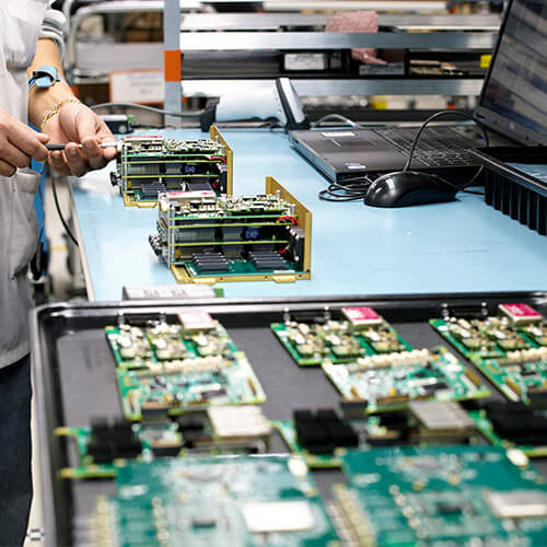
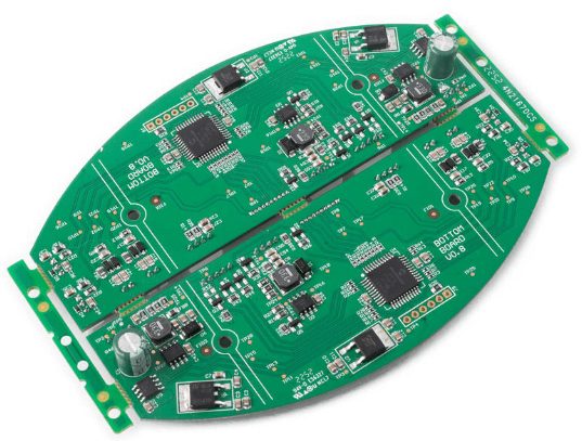
PCB Panelization, also called PCB arrays, are composed of multiple small boards arranged to form a larger unit. These panels streamline manufacturing and assembly processes. After the components are mounted, a depaneling process separates individual PCBs from the array.
These outstanding characteristics of coated and resin PCBs emphasize the necessity of analyzing the system and requirements to make the right decision. Coatings have different functions and disadvantages. The same is true for resin PCBs. To complicate matters, some devices now adopt 2K coated PCBs due to their advanced characteristics.
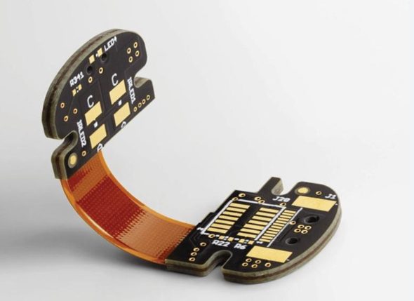
Both types of circuit boards have their own advantages and disadvantages. Rigid-flex boards are more flexible than Fr4 rigid boards. Fr4 has a higher flame retardancy. Therefore, it is used according to the current situation. Rigid-flex boards have more industrial uses, which explains why they are more expensive, while Fr4 rigid boards have more universal uses and are therefore cost-effective.
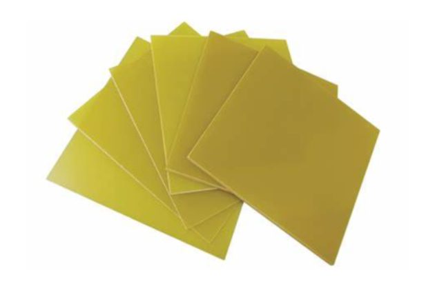
FR-4 is one of the substrate materials of PCB. The colors of FR-4 board surface include yellow FR-4, white FR-4, black FR-4, blue FR-4, etc.FR-4 is not a material, but a material grade, which represents a material code of a fire resistance grade. It means that the resin material must be able to extinguish itself after burning.
In the era of smart manufacturing, industrial robots are transforming the production landscape with enhanced efficiency, precision, and safety. Central to this evolution is the indispensable role of printed circuit boards (PCBs). Acting as the “nervous system” of robots, PCBs support signal transmission, control functions, and intelligent decision-making. As robotics technology advances, so too does the design and functionality of PCBs.


