Can flexible boards be made into 4 layer PCB?
Flexible Printed Circuit Boards (PCBs) play a crucial role in modern electronic devices, catering to diverse application requirements with varied specifications. From double-layer computer flexible PCB boards to those designed for consumer electronics and single-layer medical applications, each possesses unique designs and applications.But if you have higher requirements, you wonder if they can be made into 4-layer boards?
Can flexible PCB boards be made into 4 layer PCB?
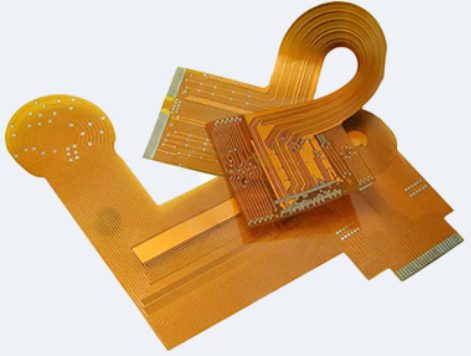
FPC flexible PCB boards can produce four-layer PCB boards, but compared to double-layer or multi-layer FPC flexible PCB boards, the manufacturing process is more complex and issues such as insulation performance, signal transmission, manufacturing processes and applications need to be considered. The four-layer FPC flexible PCB board has the advantages of high space utilization, good flexibility and light weight, and has broad application prospects in high-end electronic products.
Material properties
FPC flexible PCB board is made of polyimide film as the base material, and conductor patterns are formed through processes such as copper coating, etching, and drilling. It has good flexibility and bendability. However, due to the special structure of FPC flexible PCB boards, the manufacturing of four-layer boards is relatively complex, and the insulation between wire layers and the reliability of signal transmission need to be considered.
Insulation performance: The polyimide film as the base material of the FPC flexible PCB board has good insulation properties and can meet the insulation requirements of the four-layer board. However, during the manufacturing process, attention needs to consider the design and manufacturing of the insulation layer between the wire layers to ensure the insulation performance of the four-layer PCB board.
Signal transmission: The wire layer of the FPC flexible PCB board is made of conductive copper foil, which has good conductive properties. However, the four-layer PCB board has more wire layers and requires higher requirements for the reliability of signal transmission. Therefore, signal interference and crosstalk issues between wire layers need to be considered during the design and manufacturing process.
Manufacturing process
The process of manufacturing four-layer FPC flexible PCB boards is more complicated than that of double-layer or multi-layer FPC flexible PCB boards. It mainly includes the following aspects:
Lamination process: The four-layer FPC flexible PCB board requires multiple laminations to achieve the superposition of wire layers. During the lamination process, parameters such as temperature, pressure and time need to be controlled to ensure a strong bond between the wire layers.
Drilling process: Four-layer FPC flexible PCB boards require multiple drillings to achieve electrical connections between wire layers. The drilling process requires precise control of hole diameter and location to ensure reliable electrical connections between wire layers.
Etching process: In the manufacturing of four-layer FPC flexible PCB boards, multiple etching processes are required to form wire patterns. The etching process needs to control the concentration of the etching solution and the etching time to ensure the accuracy and quality of the conductor pattern.
Application fields
FPC flexible PCB boards are widely used in electronic products, such as mobile phones, tablet computers, automotive electronics, etc. Compared with double-layer or multi-layer FPC flexible boards, four-layer FPC flexible PCB boards can provide more wire layers, allowing for more complex circuit designs and higher signal transmission rates. Therefore, four-layer FPC flexible boards have broad application prospects in high-end electronic products.
Advantages Of Four-layer FPC flexible PCB boards
Four-layer FPC flexible PCB boards have the following advantages over traditional rigid boards or double-layer FPC flexible boards:
High space utilization: The four-layer FPC flexible PCB board can achieve more conductor layers in a limited space, thereby improving circuit integration and space utilization.
Good flexibility and bendability: FPC flexible PCB boards have good flexibility and bendability, and can adapt to complex product shapes and curved surface designs.
Light weight: Compared with traditional rigid boards, FPC flexible PCB boards are lighter and can reduce the weight of the overall product.
KKPCB’s solution on Flexible PCBs
Let’s start with the double-layer computer flexible board. With a thickness of 1.2mm and both outer and inner layers having a copper thickness of 1 ounce, it has a minimum hole size of 0.2mm and a minimum line width of 3 mil. It’s specifically engineered for computer applications, prioritizing reliability and performance in this technological realm.
Next, our consumer electronics flexible PCB board is slightly thinner at 0.8mm, featuring the same outer and inner layer copper thickness of 1 ounce. With a minimum hole size of 0.3mm and a minimum line width of 3 mil, it caters to the demands of consumer electronic devices, emphasizing a balance between flexibility and functionality.
In addition, the single-layer medical flexible PCb board stands out with a thickness of 0.6mm and a copper thickness of 1 ounce for both outer and inner layers. With a minimum hole size of 0.3mm and a minimum line width of 2 mil, it prioritizes precision and reliability, critical for medical applications where accuracy is paramount.
In terms of manufacturing capabilities, KKPCB offers a wide range of features for flexible PCBs. Our capabilities cover 1 to 10 layers with materials like DuPont or local polyimide. The PCB boards can range in thickness from 0.08mm to 0.8mm, and copper thickness from 0.5oz to 2.0oz.
Our capabilities include fine specifications like a minimum tracing and spacing of 2 mil, a minimum drilling hole diameter of 8 mil, and various solder mask and silkscreen color options. Surface treatments like immersion gold, OSP, immersion silver, and immersion tin ensure enhanced durability and functionality. Plus, their precision with a tolerance of dimension at ±0.05mm and lead times ranging from 2 to 28 days contribute to diverse applications.
Through the flexibility in design, material options, and precision engineering showcased,KKPCB’s capabilities empowers the creation of tailored flexible PCBs catering to the specific needs of various industries, from computing to consumer electronics and even critical medical devices.

