


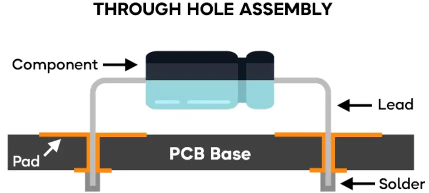
One of the two most common methods of attaching electronic components to PCBs is the through-hole or through-hole process. This technology is older than SMT, and for many years, it was the standard technology for PCB assembly. When surface mount technology became popular in the 1980s, many people thought it would make through-hole PCB assembly obsolete. However, through-hole technology has several advantages that make it still a preferred choice for certain applications.
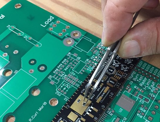
Basic soldering guide on how to solder electronic components to a printed circuit board (PCB). This is a detailed and complete soldering guide for both automated soldering in mass production and manual soldering in PCB rework and repair.
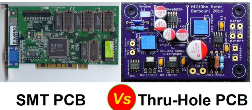
SMT vs. Through-Hole – Disadvantages of SMT vs. Through-Hole
Since not all basic electronic components are available for surface mounting, the actual area savings on the board will depend on the percentage of through-hole components replaced by surface mount components. The three types of surface mount offer varying degrees of benefit depending on the component combination.
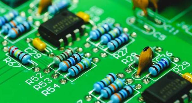
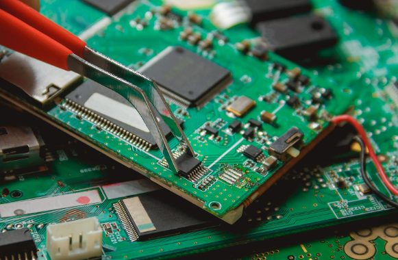
SMD soldering or surface mount technology assembly requires different SMT equipment and more experience and expertise. SMT PCBs have flat tin-lead or gold-plated copper pads without any holes. These traces are called “pads
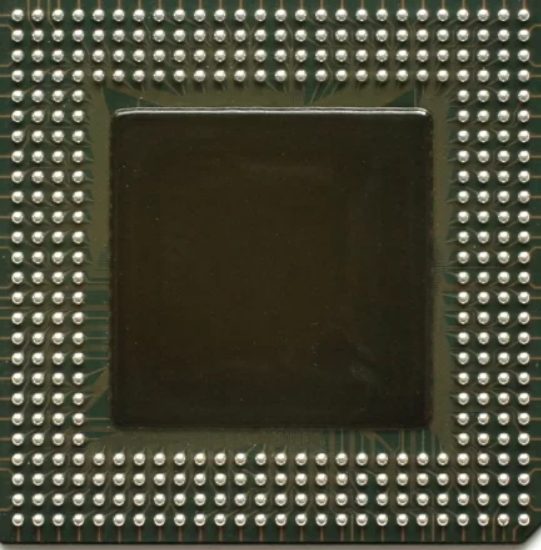
The lower thermal resistance between the BGA package and the PCB components is another advantage of this type of package. This allows heat to flow more freely, resulting in better heat dissipation and preventing the device from overheating.
Surface Mount Technology (SMT) is widely used in the PCB assembly process, but like any complex manufacturing technology, it is not immune to defects. Whether you’re dealing with solder balls, bridging, tombstoning, or unmelted solder paste, troubleshooting is a key part of ensuring high-quality SMT production.
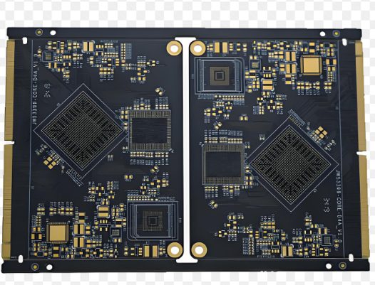
A Multilayer PCB (Printed Circuit Board) is a type of PCB with more than two conductive layers. Unlike a double-sided PCB, which has two copper layers (top and bottom), a multilayer PCB consists of three or more layers of copper, interconnected by copper-plated vias. The number of layers can range from 3 layers to 40 layers or more, depending on the design requirements
As we step into 2025, the electronics manufacturing industry is poised for transformative changes driven by technological advancements, shifting consumer demands, and global economic factors. At KKPCB, we are committed to staying at the forefront of these developments to deliver cutting-edge solutions to our clients. Here’s an overview of the key trends set to reshape the industry this year.
A Single-Sided PCB (also known as a Single-Layer PCB or One-Layer PCB) is the simplest and most cost-effective type of printed circuit board. As the name suggests, it has a single conductive layer (usually copper) on one side of the substrate, with the electronic components mounted on the opposite side.
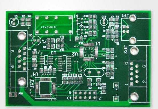
A Double-Sided PCB (also known as a Double-Layer PCB) is a type of printed circuit board where both sides of the substrate are used for placing electronic components and conductive copper traces. Unlike single-sided PCBs, which have a copper layer on only one side, double-sided PCBs feature conductive layers on both sides of the board, connected via plated-through holes (PTH), allowing circuits to connect between the top and bottom layers.