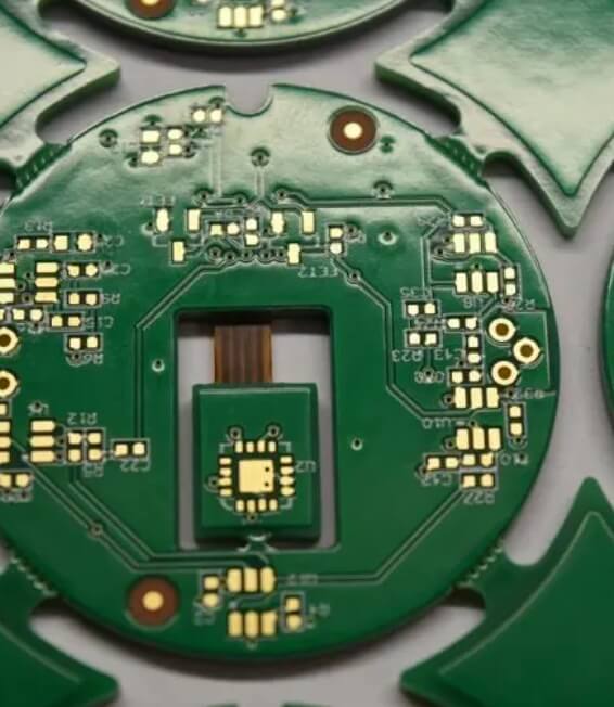
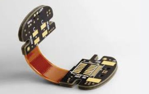
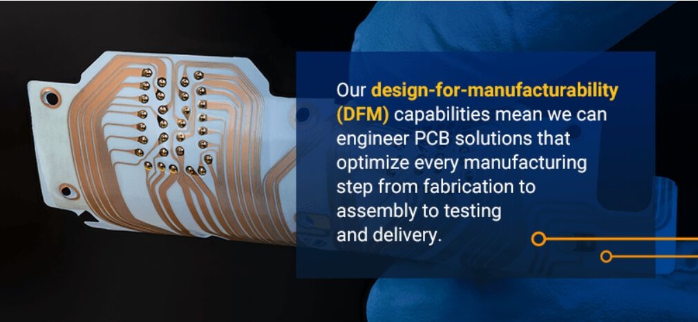
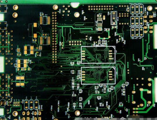
These PCBs create a more challenging design for rigid-flex manufacturers, but we’ve been able to supply successful designs with full compliance and reliability. By engineering these in a 3D environment, we’re able to achieve spatial efficiency and incorporate folds and flexes to help you meet the desired shape that works best with your application.
Rigid PCBs are inherently versatile and are suitable for a variety of configurations from single to multi-layer. With KKPCB’s design for manufacturability and engineering services, you can find a rigid PCB that matches your size, material, and build specifications.
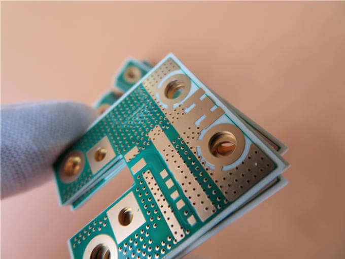
Each rigid and flexible printed circuit board (PCB) design is different and can be customized based on the purpose of the board. The same is true for the PCB substrate – fiberglass is a commonly used substrate, but aluminum-based PCBs are also very effective in many industrial applications. Aluminum-based PCBs consist of a metal-based, copper-clad laminate that provides high performance, including excellent electrical insulation and thermal conductivity.
PCB layering or stacking is a way of stacking multiple printed circuit boards together while ensuring that there are predefined interconnections between them, allowing multiple printed circuit boards to be installed in the same device. These multi-layer PCBs can multiply the speed and functionality of a device and are composed of at least three conductive layers, with the bottom layer being composited with an insulating board.
Microstrip patch antennas and their arrays may be rare but are the most widely used antenna form. They have a simple structure and can be formed by a dielectric, a metal conductor patch on the dielectric layer, and a ground plane. Even the dielectric in the middle can be an air structure. A typical microstrip patch antenna is made on a printed circuit board (PCB), and a fine line structure is etched on the conductive metal layer using a photocopying method
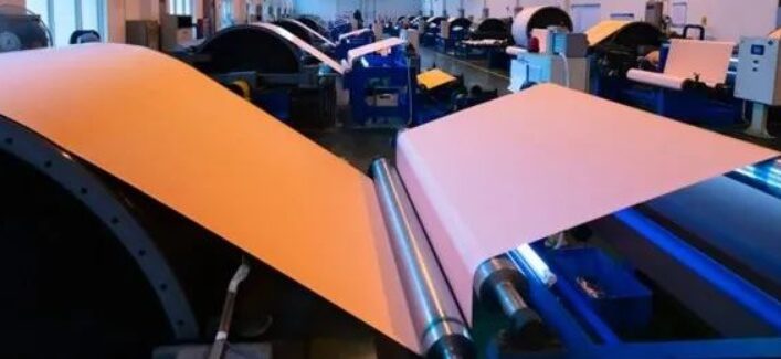
Copper foil used in the PCB industry is more complex than you might think. Copper is both an excellent conductor of electricity and an excellent conductor of heat, making it an ideal conductor for most PCB applications. Copper foil has many other properties that are important for engineers to understand.
With HDI boards, you can affix more components on both sides of the bare PCB, allowing you to get more functionality in a smaller space and expand the overall functionality of your device. HDI technology enables you to add functionality while reducing the size and weight of your product.
24GHz radar detection system mainly supports short-range detection (SRR), high frequency circuit board and high wavelength. Applicable boards: RO4835, RO4350B, RO4003C . Among them, RO4350B nitride ceramic laminate and RO4835 nitride ceramic laminate are highly recommended. These two series belong to the cost-effective series for people’s daily use.
Power Electronics: Another benefit of a flexible printed circuit board is that it can be coupled with highly flexible, thin layers of copper, which means the board can handle heavier power currents. This is especially important in devices that will require more power to operate at full capacity, like those found in the power electronics industry.
Generally, multilayer circuit boards are designed with large amounts of copper foil as grounding devices. Sometimes, the Vcc layer is also designed with large amounts of copper foil. When these large amounts of copper foil cannot be evenly distributed on the same multilayer circuit board, it will cause problems with uneven heat absorption and heat dissipation rates. The multilayer circuit board will naturally expand and contract when heated and contract when cooled. If the expansion and contraction cannot be achieved at the same time, different ground stresses will be caused and the board will deform. At this time, if the temperature of the board has reached the limit of the Tg value, the board will gradually soften and cause deformation


