


In modern electronic equipment, high-frequency PCB boards are widely used and are also an indispensable part of many high-frequency devices. Most of them are used in applications with relatively strict requirements for high-frequency PCB boards .
High-frequency PCB circuit boards are circuit boards specially designed for transmitting high-frequency signals. They have special design and manufacturing requirements to ensure good signal transmission performance and the lowest possible signal attenuation in the high-frequency range
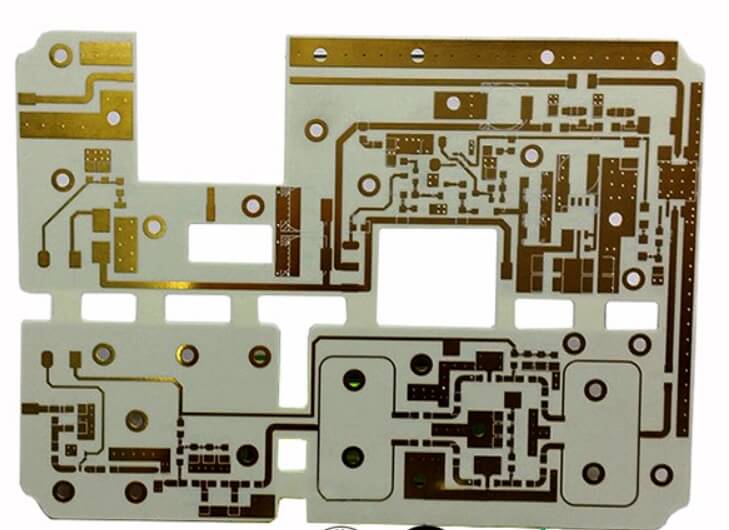
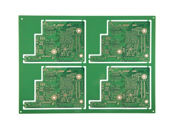
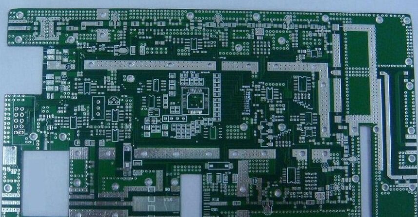
High-frequency circuit boards refer to special PCB circuit boards with higher electromagnetic frequencies. They are used in high-frequency (frequency greater than 300MHZ or wavelength less than 1 meter) and microwave (frequency greater than 3GHZ or wavelength less than 0.1 meter) fields. They are produced on microwave substrate copper-clad boards using some processes of ordinary rigid circuit board manufacturing methods or using special processing methods. Generally speaking, high-frequency boards can be defined as circuit boards with frequencies above 1GHz.
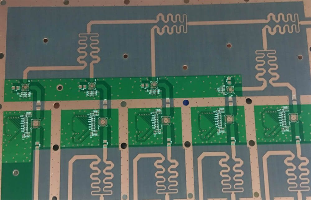
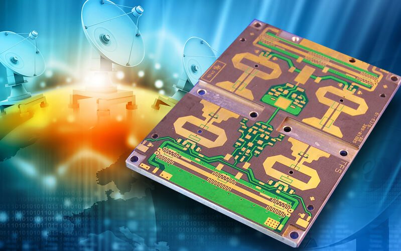
Radio frequency (RF) and microwave (MW) circuits can be found in countless wireless products, from handheld devices used in medical and industrial applications to advanced communications systems used in base stations, radar and global positioning. The success of these high-speed products begins during the product design phase when selecting PCB laminate materials
High frequency and induction heating technology currently have the highest heating efficiency and speed for metal materials, and are low-cost and environmentally friendly. It has been widely used in various industries in the heat processing, heat treatment, hot assembly, welding, smelting and other processes of metal materials
Frequency range: Generally speaking, high-frequency boards can be defined as PCBs with a frequency above 1GHz. They are mainly used in PCBs in the fields of high frequency (frequency greater than 300MHz or wavelength less than 1 meter) and microwave (frequency greater than 3GHz or wavelength less than 0.1 mete
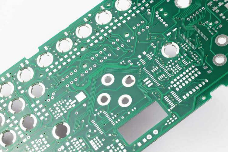
High-frequency PCB is a special circuit board with a higher electromagnetic frequency, which is above 1GHz. The physical properties, precision and technical parameters of high-frequency PCB are very high, and it is often used in radar, military equipment, aerospace and other fields.
RO4000 series laminates can be processed using standard FR-4 techniques without specialized via preparation. They are rigid, thermoset laminates, compatible with automated systems and scrubbing equipment for copper surface preparation. RO4835 laminates are RoHS compliant and suitable for UL 94V-0 certified applications.
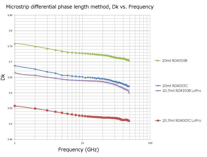
RO4000 hydrocarbon ceramic laminates are designed to offer superior high frequency PCB performance and low cost circuit fabrication. The result is a low loss material which can be fabricated using standard epoxy/glass (FR-4) processes offered at competitive prices.
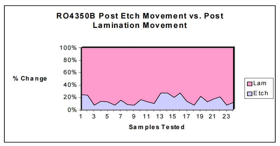
This study was conducted to evaluate dimensional movement of Rogers RO4350B
Product through the circuit fabrication process. The study was conducted using Six
Sigma tools and the DMAIC process as a guideline for the evaluation (Define, Measure,
Analyze, Improve, and Control). The Six Sigma project was initiated as a joint exercise between Rogers Corporation and printed circuit board manufacturer Cirtech Inc.