


PCB interconnections can be categorized into three main types: chip-to-PCB, interconnections within the PCB, and PCB-to-external devices. High-frequency PCB designs require addressing RF effects at these interconnection points to ensure optimal performance. This guide covers techniques for minimizing RF interference, crosstalk, and return loss across these interconnection types.
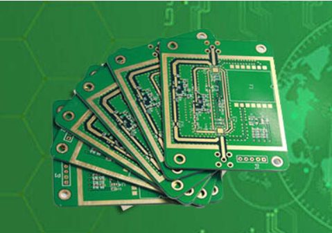
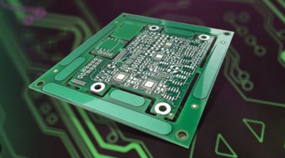
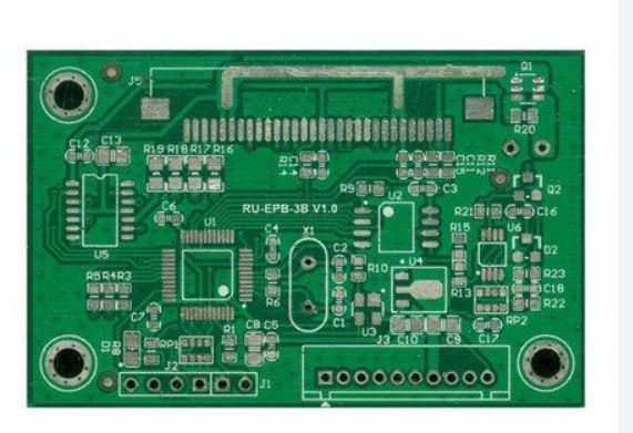
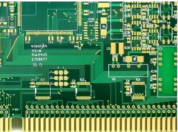
Printed circuit boards (PCBs) remain the backbone of electronic assembly across various systems. Even with perfectly designed schematics, poor PCB design can significantly compromise reliability. For instance, closely spaced thin parallel lines on a PCB can cause signal waveform delays and reflected noise at transmission line terminals. This guide outlines essential considerations for designing reliable PCBs.
Electromagnetic interference (EMI) control is critical in high-speed PCB design, and one often-overlooked aspect is the influence of integrated circuit (IC) packaging. Incorporating decoupling capacitors within the IC package can effectively reduce EMI and enhance signal integrity. This guide delves into the role of IC packaging in EMI suppression, exploring the root causes of EMI, key IC package design considerations, and practical design rules to optimize performance.
As electronic devices become increasingly miniaturized, advancements in component and wiring technologies have created new challenges for production testing. Highly integrated ICs, smaller insulation spacings, and limited access to circuit nodes have made traditional testing methods insufficient. To address these challenges, a design-for-testability (DFT) approach is essential to reduce testing costs and enhance production efficiency. This guide explores the principles, strategies, and best practices for improving PCB testability.
Understanding the classification and parameters of PCB materials is essential for selecting the right material for a specific application. Factors like flame retardancy, Tg, resin type, and base material play critical roles in the performance and reliability of PCBs.
The quality of SMT laser steel mesh depends on factors like manufacturing process, material selection, design precision, and maintenance. By adhering to best practices in cleaning, storage, and handling, you can ensure optimal stencil performance and longevity.
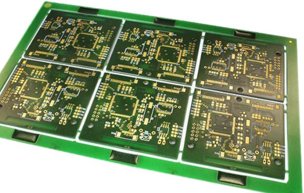
Achieving efficient automatic PCB wiring involves a blend of strategic planning, tool utilization, and manual refinement. By setting robust design rules, optimizing layout, and leveraging EDA tools effectively, engineers can create high-quality PCB designs that meet performance and manufacturability requirements. The iterative approach of routing, validating, and refining ensures that even the most complex designs achieve high routing rates and functionality.
RF (Radio Frequency) circuits and interfaces exhibit unique characteristics, requiring specialized design considerations. These challenges are due to the nature of RF signals and their interaction with physical elements of the circuit. Understanding these aspects ensures optimal performance in wireless communication systems. Below is an exploration of RF circuit characteristics, PCB design considerations, and optimization techniques.
Grounding is a critical aspect of PCB design, particularly in mixed-signal environments where digital and analog circuits coexist. Proper grounding ensures stable performance, minimizes noise, and improves the reliability of the overall circuit. Below are key insights and guidelines to address grounding challenges effectively.
In power supply design, PCB layout plays a critical role in ensuring the circuit’s efficiency, stability, and reliability. Below are five essential considerations for effective PCB design in power supply applications: