


Open circuits in PCBs can often be traced back to mechanical damage during various stages of production—whether from scratched copper clad laminate, improper handling, or worn tools. Implementing the outlined improvement methods can significantly reduce the occurrence of these issues, improving both product quality and production efficiency.
Proper PCB design requires careful planning and attention to detail, from schematic creation to component layout and wiring. Following these best practices ensures optimized signal integrity, reduces interference, and minimizes manufacturing issues, leading to higher-quality and more reliable PCB designs.
Understanding these common misunderstandings in circuit design is essential for engineers who want to improve efficiency, reduce power consumption, and design more reliable systems. By addressing these myths, you can avoid co
Electromagnetic compatibility (EMC) refers to the ability of electronic devices to function harmoniously in their electromagnetic environment without causing or being affected by electromagnetic interference (EMI). The goal of EMC design is to enable electronic devices to resist external interference while minimizing the electromagnetic interference they emit to surrounding devices
In circuit board manufacturing, various electroplating methods are employed to enhance performance, durability, and contact quality. This article focuses on four specialized electroplating methods commonly used in PCB (printed circuit board) welding processes
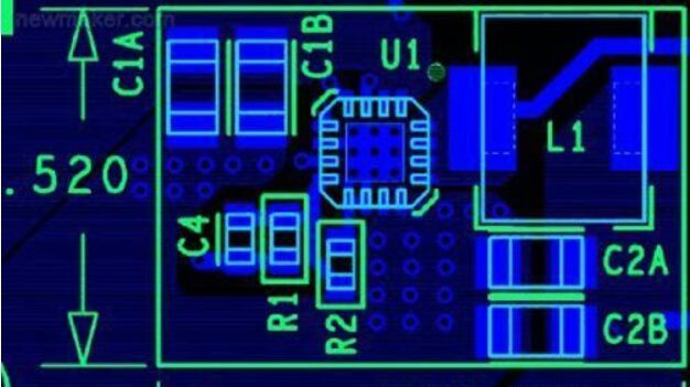
RF circuit board design is a critical and often complex area of PCB engineering. While there are many uncertainties in theory, practical design rules can be followed to optimize performance.
HDI boards represent the forefront of PCB technology, enabling smaller, more efficient electronic devices while meeting the demands of modern consumer electronics and telecommunications.
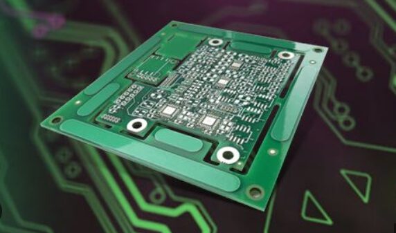
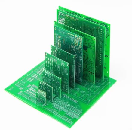
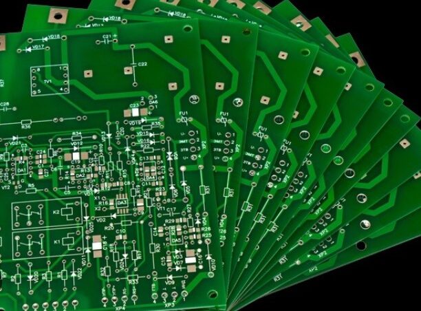
Printed Circuit Boards (PCBs) are the foundation of most electronic devices. The PCB production process can be categorized into subtractive methods and additive methods. Currently, the most commonly used industrial method is the copper foil etching process, a subtractive method.
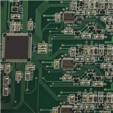
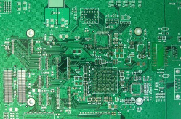
PCB design involves two critical stages: component layout and circuit connection wiring. The layout is the arrangement of circuit components within the PCB’s wiring area. A well-thought-out layout directly affects the ease of subsequent wiring and significantly impacts the PCB’s overall performance. In addition to meeting circuit functionality and performance requirements, a good layout considers manufacturability, inspection, and maintenance. Components should be placed evenly, neatly, and compactly, ensuring that leads and connections are short, minimizing interference and signal transmission delays.

It is generally recommended to use the method of automatic routing + manual adjustment. Automatic routing requires routing in the order of ground line – power line – clock line – others. Set the routing priority in the routing rules, 0 is the lowest level, 100 is the highest level, and there are 101 situations in total. In more complex circuit boards, considering the requirements of electrical characteristics, interference and other factors, we all use manual routing. It is forbidden to place vias on the pins of components, and the already routed lines should be locked before automatic routing. The routing should take into account both aesthetics and electrical characteristics. In particular, the routing that affects the appearance should be routed on the reverse side. In principle, do not route the front side of the product name, model and Zhongyou logo (except in special cases), and do not allow front routing between the silk screen frame and the Keepout frame (except in special cases).