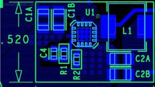
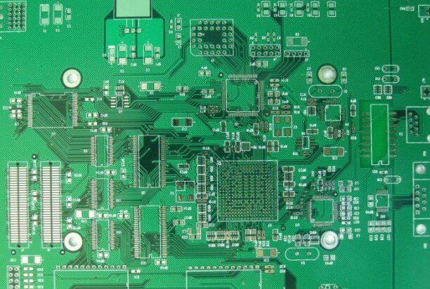
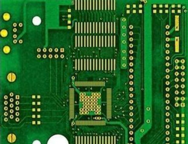
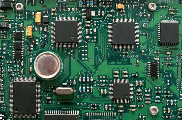
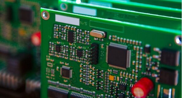
PCB design involves two critical stages: component layout and circuit connection wiring. The layout is the arrangement of circuit components within the PCB’s wiring area. A well-thought-out layout directly affects the ease of subsequent wiring and significantly impacts the PCB’s overall performance. In addition to meeting circuit functionality and performance requirements, a good layout considers manufacturability, inspection, and maintenance. Components should be placed evenly, neatly, and compactly, ensuring that leads and connections are short, minimizing interference and signal transmission delays.
It is generally recommended to use the method of automatic routing + manual adjustment. Automatic routing requires routing in the order of ground line – power line – clock line – others. Set the routing priority in the routing rules, 0 is the lowest level, 100 is the highest level, and there are 101 situations in total. In more complex circuit boards, considering the requirements of electrical characteristics, interference and other factors, we all use manual routing. It is forbidden to place vias on the pins of components, and the already routed lines should be locked before automatic routing. The routing should take into account both aesthetics and electrical characteristics. In particular, the routing that affects the appearance should be routed on the reverse side. In principle, do not route the front side of the product name, model and Zhongyou logo (except in special cases), and do not allow front routing between the silk screen frame and the Keepout frame (except in special cases).
At KKPCB, we offer reliable electronic components sourcing, streamlining the process for you. Send us your BOM, and we’ll handle everything, eliminating the need for you to compare prices and sources.
HDI board is the abbreviation of High Density Inverter. It is a kind of (technology) for producing printed circuit boards. It is a circuit board with relatively high line distribution density using micro blind buried hole technology. HDI board is a compact product designed for small-capacity users. It adopts modular parallel design. One module has a capacity of 1000VA (height 1U), natural cooling, and can be directly placed in a 19″ rack. Up to 6 modules can be connected in parallel. This product adopts full digital signal process control (DSP) technology and multiple patented technologies. It has full range of load adaptability and strong short-term overload capacity, and can ignore the load power factor and peak factor.
In fact, there is no clear definition of HDI high-density manufacturing method, but generally there is a big difference between HDI and non-HDI. First of all, the aperture used in the circuit carrier made of HDI must be less than or equal to 6mil (1/1,000 inch), and the ring diameter of the hole ring must be ≦10mil, and the layout density of the line contacts must be greater than 130 points per square inch, and the line spacing of the signal line must be less than 3mil.
When discussing wiring-related technologies, two issues will be discussed: What if management cannot use a double-layer board or a ground plane, but still needs to reduce the noise in the circuit? And how to design the circuit to meet the ground plane requirements? Generally speaking, the solution is to tell management that a ground plane is necessary if reliable circuit performance is to be achieved. The main reason for using a ground plane is that the ground impedance is low and it can reduce EMI to a certain extent. But if cost constraints prevent users from achieving what they need, some suggestions provided in this article, such as star networks and correct current return paths, can also slightly reduce circuit noise.
N4800-20 is a high-performance enhanced epoxy systems for multilayer PCBs requiring maximum thermal and stable electrical performance. It is designed to be lead-free assembly compatible and CAF resistant.
Gangrou combined with print circuit boards allows you to have the advantages of both the beauty. The rigid soft combination of PCB combines the flexibility of the flexible circuit and the durability of the rigid PCB. Flexible printing circuit boards are only flexible materials, which are usually based on polyimide or polyester. They can be single, double or multi -layer boards. The rigid soft combination of PCB also uses flexible and rigid materials. The flexible layer is sandwiched between the rigid layer. The rigid layer has conductors and plating holes to connect the flexible layer to other layers.
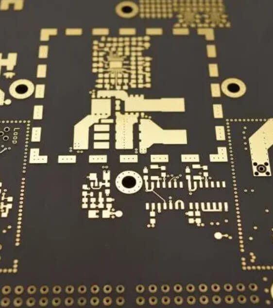
RF and microwave signals are very sensitive to noise -much more sensitive than high -speed digital signals. This means that you need to minimize the noise, bell, and reflection, and at the same time be careful to deal with the entire system.
Returning the signal with the least inductance -the ground floor below the signal will be easier to ensure this path.
Discipline matching is important. With the rise of RF and microwave frequency, the tolerance will become smaller. Generally, the PCB drive needs to be fixed, such as 50 ohms, which means that during the transmission and sending to the receiver, the drive outputs 50 ohms.
The transmission line that is curved due to wiring restrictions should use a curved radius that is at least three times larger than the central conductor width. This will minimize characteristic impedance.
It is necessary to minimize the return loss, whether it is reflected by the signal or the bell. There will always be a return path, but your design should guide it and prevent the return from multi -layer leakage through the PCB.
HDI PCBs have a higher density per unit circuit than traditional PCBs. They use a combination of buried and blind vias and microvias (0.006 inches in diameter or less). A high-density board is a PCB that has one or more of the following features:
PCB layering or stacking is a way of stacking multiple printed circuit boards together while ensuring that there are predefined interconnections between them, allowing multiple printed circuit boards to be installed in the same device. These multi-layer PCBs can multiply the speed and functionality of a device and are composed of at least three conductive layers, with the bottom layer being composited with an insulating board


