


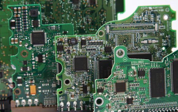
Creating a robust component library is one of the most challenging yet critical aspects of PCB design. The quality of the library, which includes schematic symbols, PCB footprints, and 3D models, directly impacts the success of your board development. Among these, the PCB footprint plays a pivotal role in determining whether your board can be manufactured and assembled correctly.
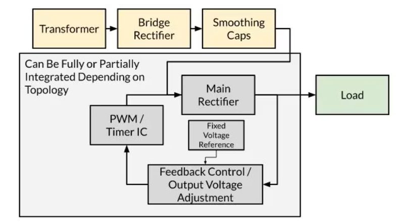
Unlike fixed power supplies that provide a constant output voltage, variable power supplies can be adjusted to different output voltages as needed. In contrast, fixed voltage power supplies or battery chargers provide a single, unchanging output voltage and are designed for specific, consistent power requirements. Read on as we discuss variable power supply PCB layout tips.
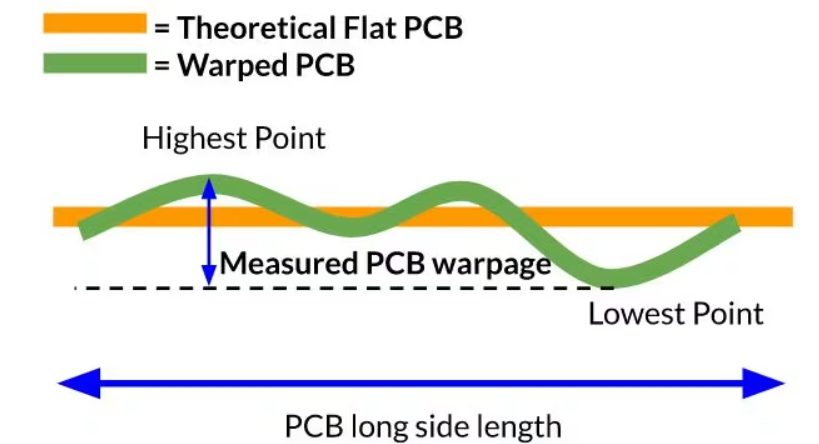
PCB warpage is a common issue caused by stress during the PCB construction process, where the board undergoes expansion and contraction, leading to internal stress and deformation. Detecting PCB warpage early in the assembly stage is crucial, as it can negatively impact printing, mounting, and soldering processes.
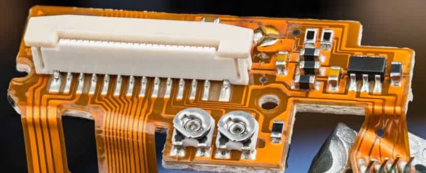
As the demand for more compact, reliable, and flexible electronic devices grows, rigid-flex PCBs are becoming increasingly popular. These boards combine the best of both rigid and flexible circuits, offering unique advantages such as enhanced durability, reduced package size, and fewer connectors.
In high-speed and RF PCB designs, controlling trace impedance is critical, but the role of RF via transitions is often underestimated. Vias, which connect signals between layers, can introduce impedance mismatches, signal reflections, and losses, especially at high frequencies. Proper design and optimization of via transitions are essential to maintain signal integrity and ensure reliable performance in RF and high-speed digital applications
Low power circuit design includes strategies focused on minimizing both dynamic and static power usage in your printed circuit boards. While selecting components with low power requirements is a crucial element, low power PCB design involves more comprehensive considerations to effectively manage power consumption.
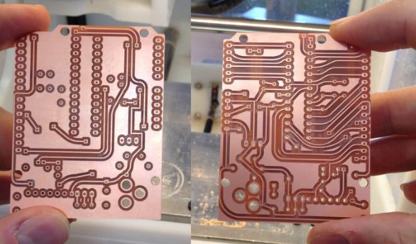
Designing double-sided PCBs requires careful planning to ensure efficient assembly, high yields, and reliable solder joints. Solder paste application and stencil design play a critical role in achieving these goals. This article explores key considerations for solder paste and stencil design, focusing on double-sided PCBs, component orientation, and advanced techniques for fine-pitch devices.

Military and aerospace PCBs must adhere to intensely high standards to ensure their safety and functionality in the extreme conditions they’re used in. For this reason, PCB design for military and aerospace applications requires incredibly stringent guidelines with built in redundancy, extra safety, and stringent tolerances, minimizing risk of failure
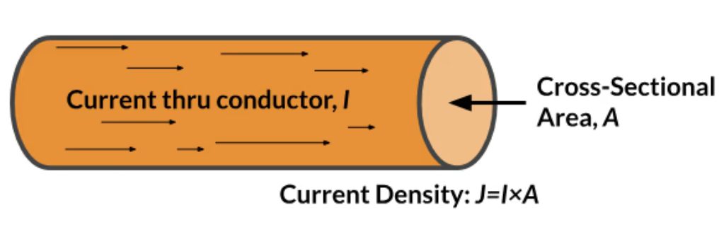
Copper current density refers to the amount of continuous current going through a copper wire —whether on a circuit board as a trace or not. According to the principles of Joule or Ohmic heating (represented as VI or I²R), any material that conducts electricity will generate heat, leading to a gradual rise in temperature in both the conductor and its surrounding environment.
When designing a printed circuit board (PCB), engineers often focus on ensuring the correct impedance structures and electrical performance of the board. However, the physical characteristics, such as PCB thickness, are equally important and can significantly impact the cost, manufacturability, and performance of the final product. While standard PCB thicknesses are widely used, they are more of a convention than a strict requirement, offering designers an opportunity for optimization, especially in high-volume production.