


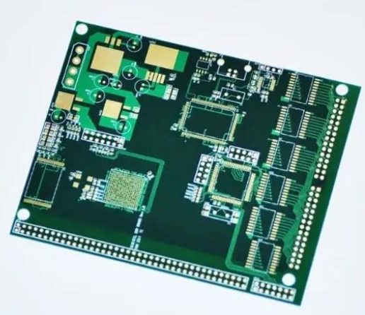
PCB design requires understanding physical processes and careful organization of layers, power networks, and signal paths. Following these recommendations reduces noise risk, improves reliability, and simplifies the routing of complex systems
When designing high-speed PCBs, the layer stack-up plays a crucial role in ensuring signal integrity, minimizing crosstalk, and achieving optimal electromagnetic compatibility (EMC). For a standard six-layer board with a thickness of 1.6mm, selecting the right structure can significantly impact performance. Below is an analysis of common six-layer board structures and their suitability for high-speed designs
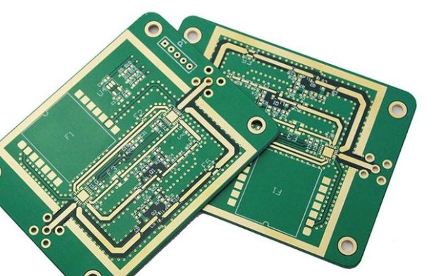
Impedance line routing in multi-layer PCBs is both an art and a science. Adhering to the principles of short lines, symmetry, equal length, and precise compensation ensures high-speed data transmission and robust device performance. By leveraging tools like the Polar Si9000 and applying best practices in design, engineers can effectively address challenges in modern PCB impedance routing.
Closely spaced vias are a common design challenge in multi-layer and high-speed PCB boards. Understanding the implications of tight spacing—such as drilling process inefficiencies, reduced solder ring size, and long-term reliability concerns—is essential. By adhering to recommended spacing guidelines, optimizing via placement, and collaborating with manufacturers, designers can enhance production yield, reduce costs, and ensure robust product per
Addressing power supply noise interference in PCB design involves a systematic approach to layout optimization, filtering, and grounding. By understanding the root causes of power supply noise and applying the countermeasures outlined above, designers can significantly enhance circuit performance and reliability. A clean power supply, well-isolated signal paths, and proper filtering are key to achieving a noise-resilient PCB.
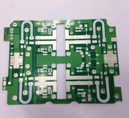
In this context, ROGERS has introduced the RO4830™ material, which, with its excellent performance and lower cost, has become a key solution in driving the widespread adoption of 77 GHz millimeter-wave radar technology.
Careful adherence to these guidelines ensures efficient and reliable mobile phone PCB designs. By prioritizing critical signal paths, ensuring proper grounding, and optimizing power distribution, potential risks in wiring are mitigated, resulting in better performance and reduced EMI issues.
Incorporating schematic simulation into the PCB design process not only saves valuable time but also increases the accuracy and efficiency of the entire workflow. By automating the process of checking for errors and verifying connections, designers can improve the overall quality of the PCB and minimize the chances of issues in the final design.
By adhering to these guidelines, engineers can ensure their PCB designs are manufacturable and optimized for high-quality production. These precautions and design considerations help reduce production errors, improve yield, and ensure the integrity of the final product.
When applied correctly, copper coating offers more benefits than drawbacks, providing improved performance, noise reduction, and thermal management for PCBs. However, to achieve the best results, it’s crucial to carefully consider the design, including grounding, copper areas, and the specific requirements of high-frequency or low-frequency circuits. By paying attention to these details, designers can optimize the copper coating for better overall performance.