Careful adherence to these guidelines ensures efficient and reliable mobile phone PCB designs. By prioritizing critical signal paths, ensuring proper grounding, and optimizing power distribution, potential risks in wiring are mitigated, resulting in better performance and reduced EMI issues.
Incorporating schematic simulation into the PCB design process not only saves valuable time but also increases the accuracy and efficiency of the entire workflow. By automating the process of checking for errors and verifying connections, designers can improve the overall quality of the PCB and minimize the chances of issues in the final design.
By adhering to these guidelines, engineers can ensure their PCB designs are manufacturable and optimized for high-quality production. These precautions and design considerations help reduce production errors, improve yield, and ensure the integrity of the final product.
When applied correctly, copper coating offers more benefits than drawbacks, providing improved performance, noise reduction, and thermal management for PCBs. However, to achieve the best results, it’s crucial to carefully consider the design, including grounding, copper areas, and the specific requirements of high-frequency or low-frequency circuits. By paying attention to these details, designers can optimize the copper coating for better overall performance.
Effective anti-interference design in PCBs and MCUs involves combining hardware measures (e.g., grounding, decoupling) and software strategies (e.g., watchdogs, error-checking). By addressing interference sources, propagation paths, and sensitive devices, you can significantly enhance circuit reliability and performance.
PCB design is a delicate balance of electrical and thermal considerations, with the relationship between current and line width being a cornerstone of reliable circuit functionality. While many empirical formulas, tables, and software tools exist online to guide this aspect of design, this article consolidates the most useful references to assist engineers in optimizing PCB layouts.
Impedance plays a critical role in the functionality, reliability, and performance of printed circuit boards (PCBs). Understanding and managing impedance is essential for ensuring proper signal transmission and maintaining the integrity of the electronic devices that rely on these boards. Below is a detailed analysis of impedance and its importance in PCB design and manufacturing.
High-speed PCB design is crucial in fields like communication, computing, and graphics/image processing. Engineers in these areas often employ unique strategies tailored to their industry’s specific requirements. Below, we explore different approaches and key considerations for high-speed PCB design.
When designing high-speed PCBs, understanding the core concepts is crucial for ensuring efficiency and functionality. This guide introduces key elements such as layers, vias, pads, and more to help beginners and professionals alike.
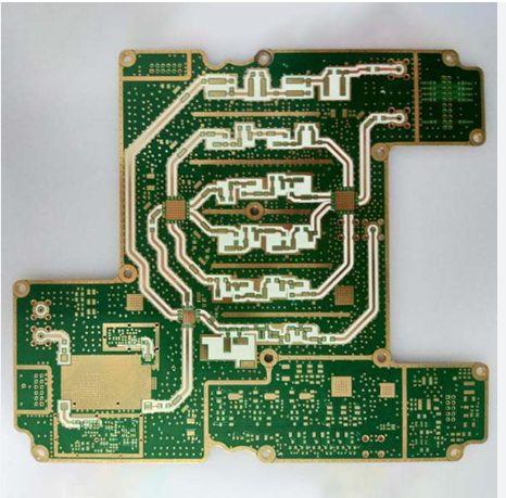
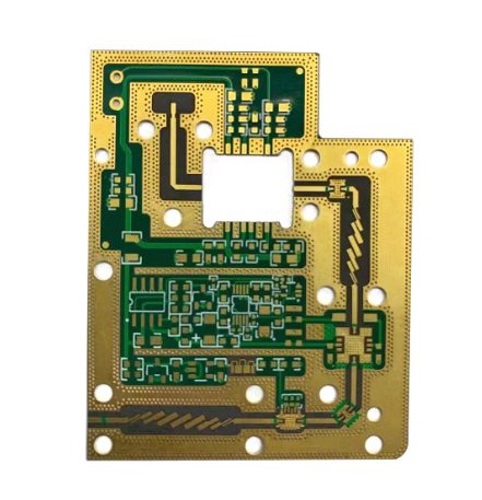
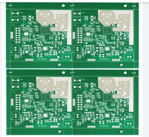
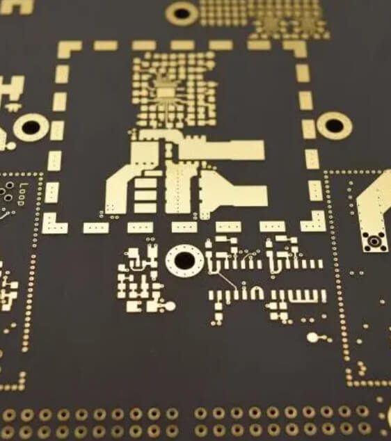
Solution Refinement and Layout: As the demand for smaller and more portable electronic devices continues to grow, the design of RF and microwave circuits is shifting towards more compact and efficient solutions. In high-frequency circuit design, the choice of PCB materials is crucial for determining circuit size, performance, and signal propagation characteristics. RT/duroid® 6010.2LM, a […]


