


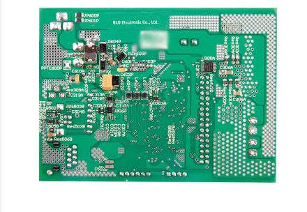
Surface Mount Technology (SMT) board assembly is a critical and widely used process in modern PCB manufacturing. This process involves placing and soldering electronic components directly onto the surface of PCB pads.
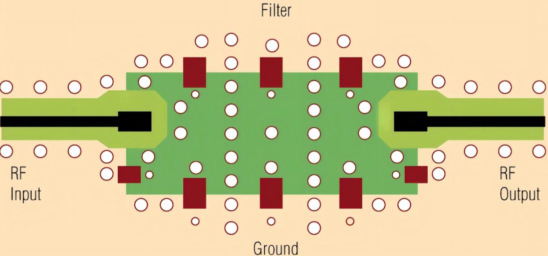
RF PCB refers to a Radio Frequency Printed Circuit Board, operating within a frequency range of 100 MHz to 100 GHz. These specialized PCBs are integral to devices that rely on wireless communication for data transfer.
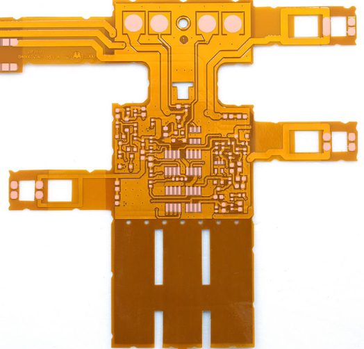
Flexible printed circuit boards (PCBs) are a cornerstone of modern electronics, found in devices like smartphones, cameras, and electric vehicles. Unlike traditional rigid PCBs made from FR4 (flame retardant material), flexible PCBs utilize polymer substrates such as polyimide, resulting in their signature amber or orange appearance
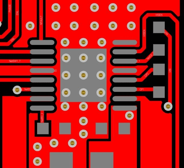
Motor driver ICs handle high currents and dissipate substantial heat, so efficient PCB design is essential to ensure proper heat dissipation and reliable performance. Below are some best practices for designing a robust PCB for motor driver ICs.
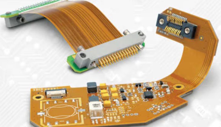
Flexible PCBs (printed circuit boards) provide the ability to bend and conform to various shapes, making them an essential technology for space-constrained and dynamic applications. A 2-layer flex PCB contains a flexible dielectric layer sandwiched between two conductive copper layers. Designing these PCBs requires unique considerations, including material selection, layout techniques, manufacturability, and reliability.
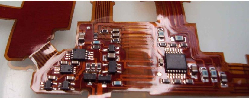
Flexible printed circuit boards (flexible PCBs or flex circuits) are made from flexible insulating materials such as polyimide film. Unlike traditional rigid PCBs, flexible PCBs can bend and twist while maintaining electrical connectivity, making them ideal for space-constrained and dynamic applications.
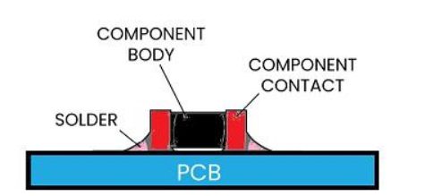
Surface mount technology is a method of assembling electronic components onto a printed circuit board (PCB). Unlike traditional through-hole technology, where the leads of the component are inserted through holes in the PCB, SMT involves mounting the component directly onto the surface of the PCB. SMT offers advantages such as smaller size, higher manufacturing efficiency, and compatibility with automated assembly processes.
The application of solder paste is one of the most crucial processes in the SMT assembly. This process requires careful attention and a high level of precision. This is because the main goal is to apply solder in the proper location and adequately. Therefore, it is important to carefully coat each pad using the appropriate amount of solder.
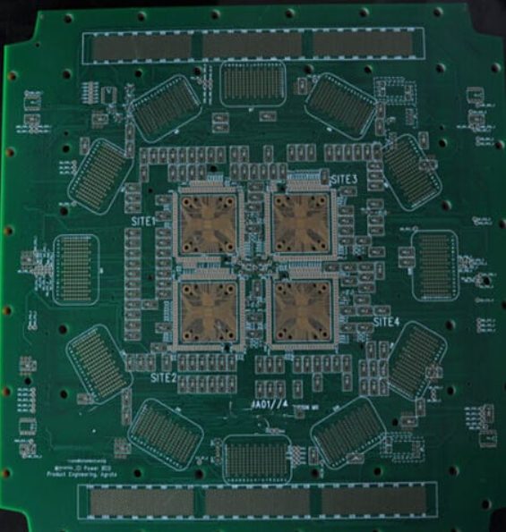
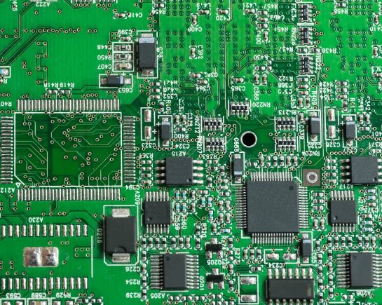
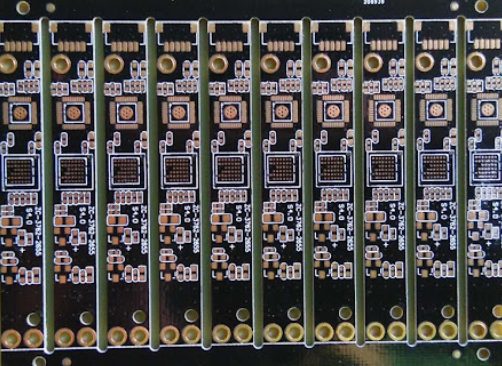
Printed circuit boards (PCBs) serve as the foundation for electronics, providing the mechanical structure and electrical connections between components. PCB fabrication involves many steps, including printing conductive traces, solder mask, legend, and other features onto the bare boards.
Printed Circuit Board (PCB) manufacturing is a complex process that involves multiple steps, one of which is the application of solder paste or other materials onto the board. This is often accomplished through screen printing, a technique that requires a high-quality stencil. The PCB screen printing stencil making process is a crucial part of PCB assembly, as it directly affects the quality and reliability of the final product