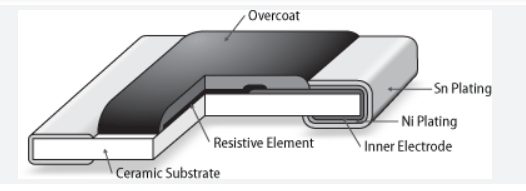
Thin film resistors have a metallic film that is vacuum deposited on an insulating substrate. Thick film resistors are produced by firing a special paste onto the substrate. The paste is mixture of glass and metal oxides. Thin film is more accurate, has better temperature coefficient and is more stable.
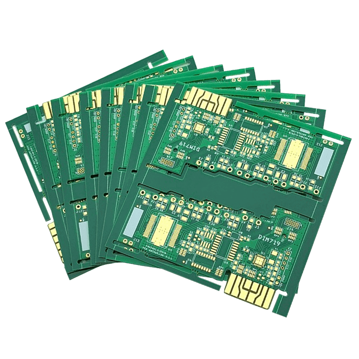
Printed circuit board (PCB) Prototyping allows engineers to check whether the design will perform as their expectations. At the same time, your PCB prototyping manufacturer would like to check if your circuit boards can be manufactured efficiently. Multiple prototyping runs can be used to test the PCB design variations or to perfect a single function before moving on to the afterwards PCB production stage.
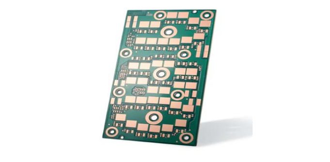
Aluminum PCB, or Aluminium PCB, also called Alu PCB, is one of Insulated Metal Substrate (IMS) PCBs, and is also one of the most commonly used Metal Core PCBs nowadays
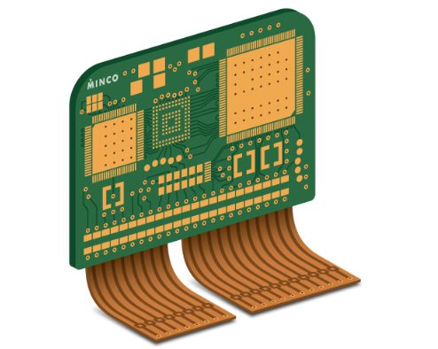
Flexible Printed Circuits (FPCs), also called Flexible Circuits, or Flex Circuits, by IPC definition, a flexible printed circuit is a patterned arrangement of printed circuitry and components that utilizes flexible based material with or without flexible cover lay. This definition is accurate, and conveys some of the potential given the available variations in base materials, conductor materials, and protective cover materials
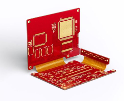
Rigid-Flex boards are a combination of rigid boards and flexible circuits that are permanently laminated together and interconnected through through-holes. Rigid-Flex boards are also written as Flex-Rigid. Rigid-Flex boards straddle the boundaries of traditional rigid boards and the unique properties of flexible circuits, using highly ductile ED or RA copper photolithography onto a flexible insulating film
High-density interconnect (HDI) PCBs are characterized by finer lines, closer spaces, and more dense wiring, which allow for a faster connection while reducing the size and bulk of a project. These boards also feature blind and buried vias, laser ablated microvias, sequential lamination, and via in-pads.
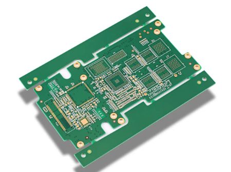
Multilayer Printed Circuit Boards (PCBs) or Multilayer Boards (MLBs) feature more than two copper layers, interconnected using copper-plated holes. These holes may include NC vias, laser microvias, through-holes, buried, or blind vias. The layers consist of copper foil, prepreg (PP), or adhesive materials and are pressed together under high temperature and pressure. This process removes air and cures the thermosetting adhesives, forming a cohesive multilayer PCB
Electronic devices have transformed modern life, and at the heart of these innovations lies a critical component: the Printed Circuit Board (PCB). From smartphones and laptops to industrial machinery and household appliances, PCBs are the backbone of electronics, enabling functionality, precision, and reliability. What Is a PCB? A Printed Circuit Board (PCB) is a thin […]
A multilayer PCB, or Printed Circuit Board, is an advanced type of circuitry that facilitates complex electronic functionalities within a compact framework.
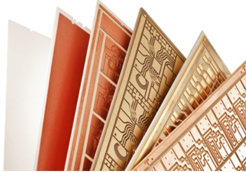
The Curamik® product suite offers best-in-class metallized ceramic substrates for higher power efficiency. Composed of pure copper bonded or brazed to a ceramic substrate, our curamik® substrates are designed to carry higher currents, provide higher voltage isolation, and operate over a wide temperature range.


