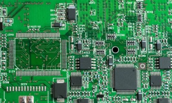
Printed Circuit Boards (PCBs) are the backbone of all electronic devices, akin to how cells are the foundation of the human body. As the structural framework of every electronic product, PCBs must be efficient and well-constructed.
When it comes to assembling Printed Circuit Boards (PCBs), there are two primary technologies: Surface Mount Technology (SMT) assembly and Through-Hole Technology (PTH) assembly
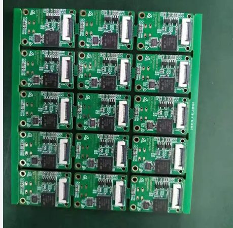
Fast Turn PCBs are printed circuit boards manufactured and assembled in a short time frame. This process is widely adopted by electronics companies because it ensures high-quality products while being cost-effective and time-efficient.
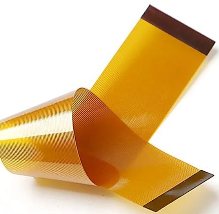
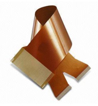
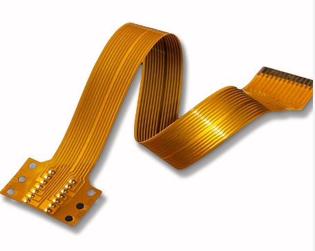
Printed Circuit Boards (PCBs) are the backbone of electronic devices, connecting components seamlessly for reliable functionality. Among these, Flexible LED PCBs have gained prominence due to their adaptability, reduced size, and cost-effectiveness compared to rigid PCBs. They are widely used across industries like consumer electronics, automotive, and aerospace
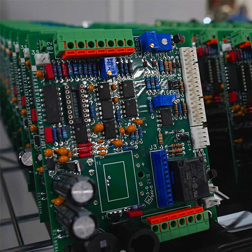
Printed circuit board (PCB) assembly is at the heart of electronic components and gadgets. Designers typically choose between two primary techniques for mounting components on PCBs: SMT (Surface Mount Technology) and PTH (Plated Through Hole).
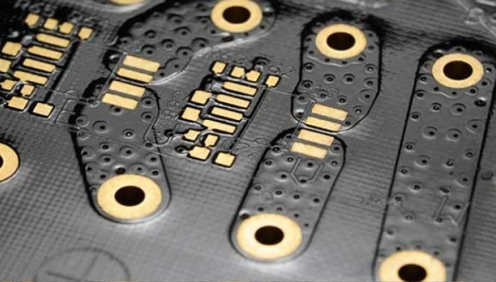
An annular ring refers to the area of copper that surrounds the drilled hole (via) in a PCB. In multi-layer PCBs, vias are essential for connecting various layers. The annular ring ensures strong electrical conductivity between these layers, as it provides the necessary copper coverage around the hole.
The introduction of phenolic resin-based laminates in the 1930s improved mechanical stability and insulation. However, the game-changer was the development of glass-reinforced epoxy laminates (FR-4) in 1940, offering superior electrical insulation, moisture resistance, and mechanical durability.
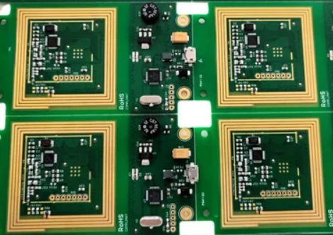
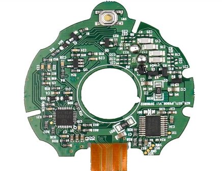
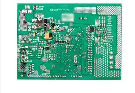
A PCB is a substrate or laminate that supports and connects electronic components to enable various device functionalities. Common substrates include FR4 (flame retardant material), but there are alternatives such as polyimide for flexible designs. PCBs are categorized by layers—single-sided, double-sided, and multi-layer—and by substrate type (rigid, flexible, or rigid-flex combinations)
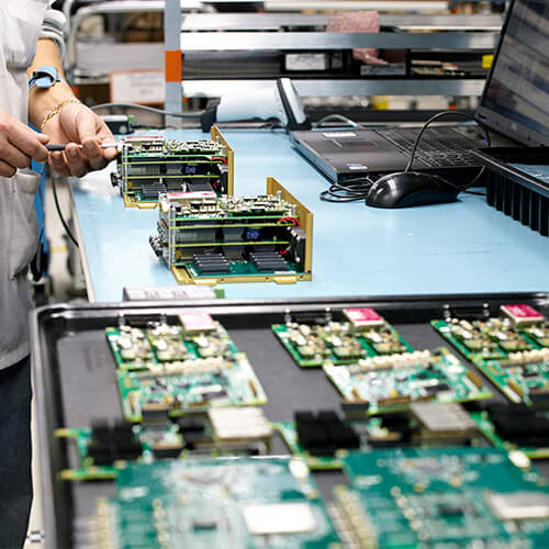
Surface Mount Technology (SMT) board assembly is a critical and widely used process in modern PCB manufacturing. This process involves placing and soldering electronic components directly onto the surface of PCB pads.
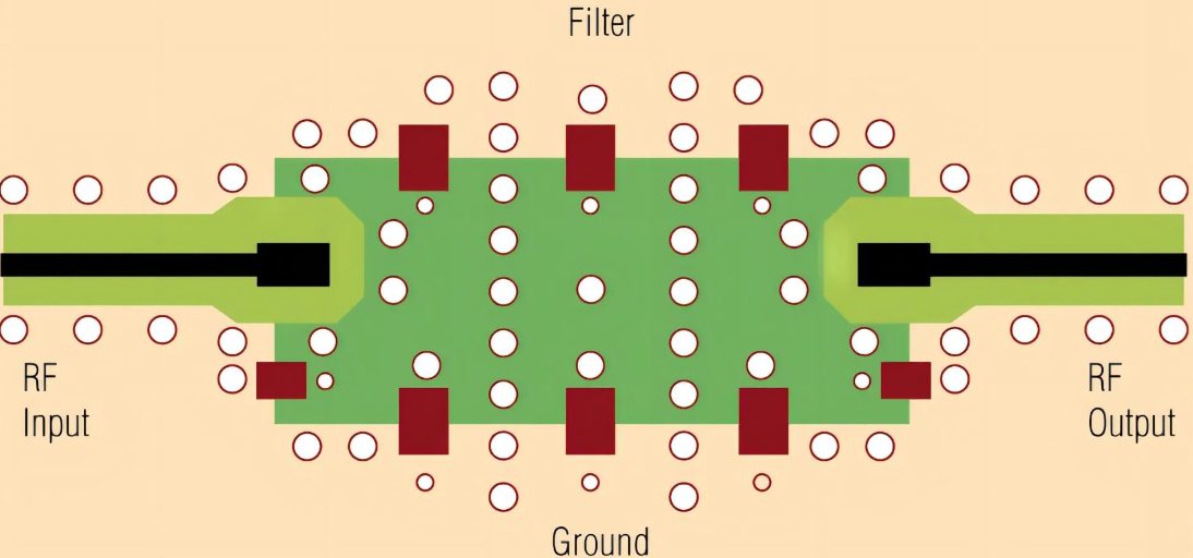
RF PCB refers to a Radio Frequency Printed Circuit Board, operating within a frequency range of 100 MHz to 100 GHz. These specialized PCBs are integral to devices that rely on wireless communication for data transfer.


