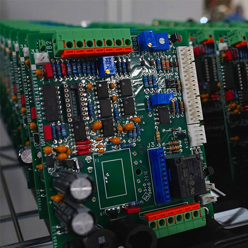
Printed circuit board (PCB) assembly is at the heart of electronic components and gadgets. Designers typically choose between two primary techniques for mounting components on PCBs: SMT (Surface Mount Technology) and PTH (Plated Through Hole).
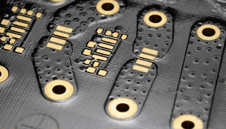
An annular ring refers to the area of copper that surrounds the drilled hole (via) in a PCB. In multi-layer PCBs, vias are essential for connecting various layers. The annular ring ensures strong electrical conductivity between these layers, as it provides the necessary copper coverage around the hole.
The introduction of phenolic resin-based laminates in the 1930s improved mechanical stability and insulation. However, the game-changer was the development of glass-reinforced epoxy laminates (FR-4) in 1940, offering superior electrical insulation, moisture resistance, and mechanical durability.
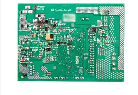
A PCB is a substrate or laminate that supports and connects electronic components to enable various device functionalities. Common substrates include FR4 (flame retardant material), but there are alternatives such as polyimide for flexible designs. PCBs are categorized by layers—single-sided, double-sided, and multi-layer—and by substrate type (rigid, flexible, or rigid-flex combinations)
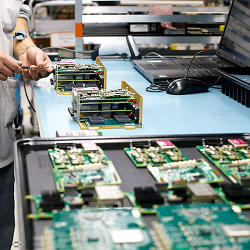
Surface Mount Technology (SMT) board assembly is a critical and widely used process in modern PCB manufacturing. This process involves placing and soldering electronic components directly onto the surface of PCB pads.
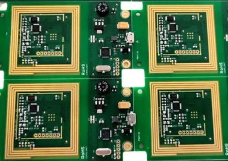
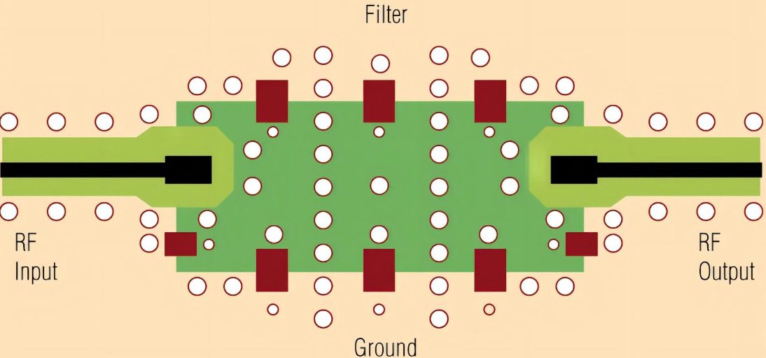
RF PCB refers to a Radio Frequency Printed Circuit Board, operating within a frequency range of 100 MHz to 100 GHz. These specialized PCBs are integral to devices that rely on wireless communication for data transfer.
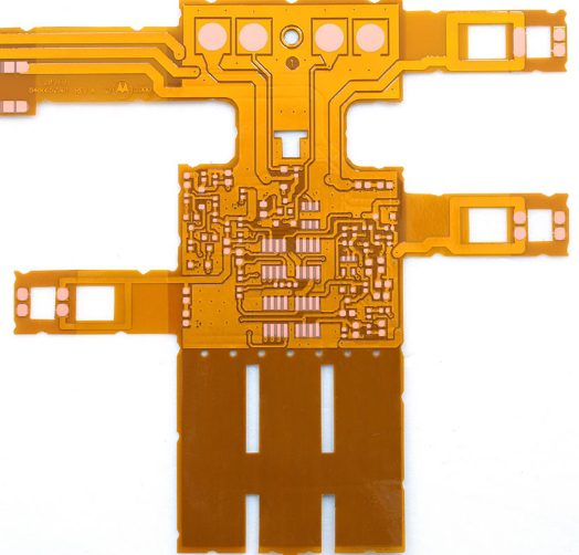
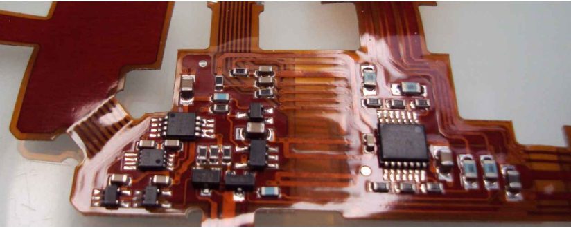
Flexible printed circuit boards (PCBs) are a cornerstone of modern electronics, found in devices like smartphones, cameras, and electric vehicles. Unlike traditional rigid PCBs made from FR4 (flame retardant material), flexible PCBs utilize polymer substrates such as polyimide, resulting in their signature amber or orange appearance
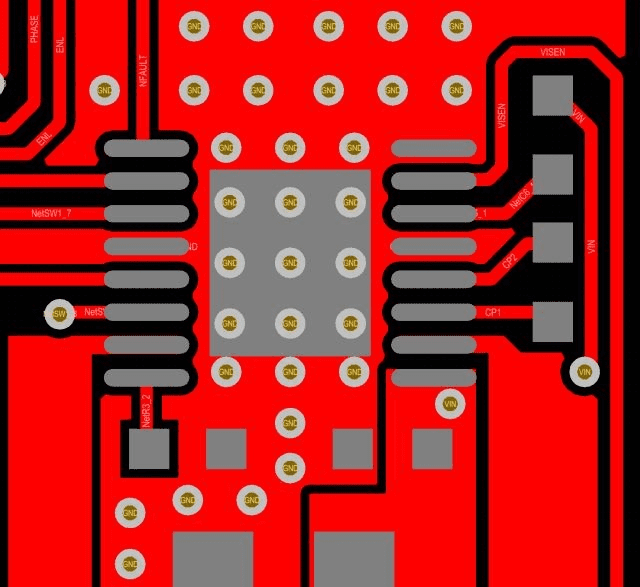
Motor driver ICs handle high currents and dissipate substantial heat, so efficient PCB design is essential to ensure proper heat dissipation and reliable performance. Below are some best practices for designing a robust PCB for motor driver ICs.
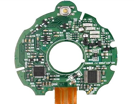
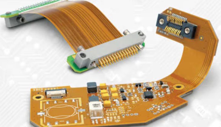
Flexible PCBs (printed circuit boards) provide the ability to bend and conform to various shapes, making them an essential technology for space-constrained and dynamic applications. A 2-layer flex PCB contains a flexible dielectric layer sandwiched between two conductive copper layers. Designing these PCBs requires unique considerations, including material selection, layout techniques, manufacturability, and reliability.
Flexible printed circuit boards (flexible PCBs or flex circuits) are made from flexible insulating materials such as polyimide film. Unlike traditional rigid PCBs, flexible PCBs can bend and twist while maintaining electrical connectivity, making them ideal for space-constrained and dynamic applications.


