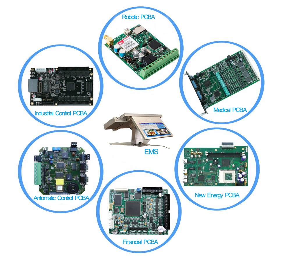
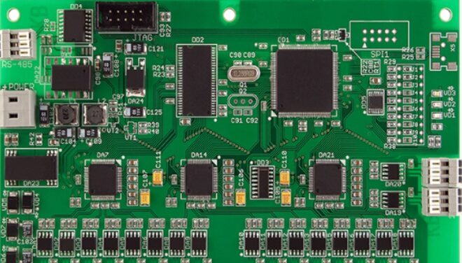
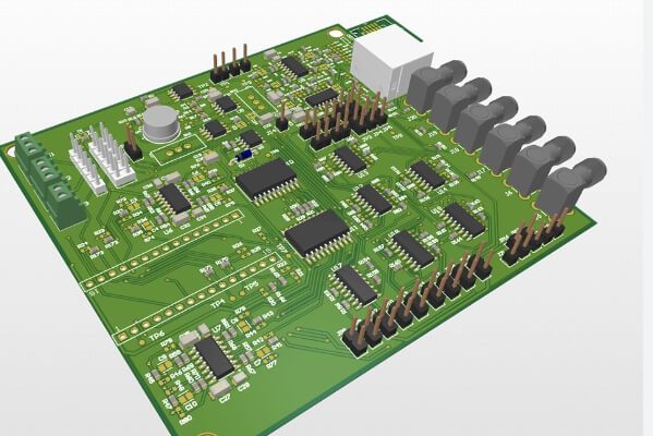
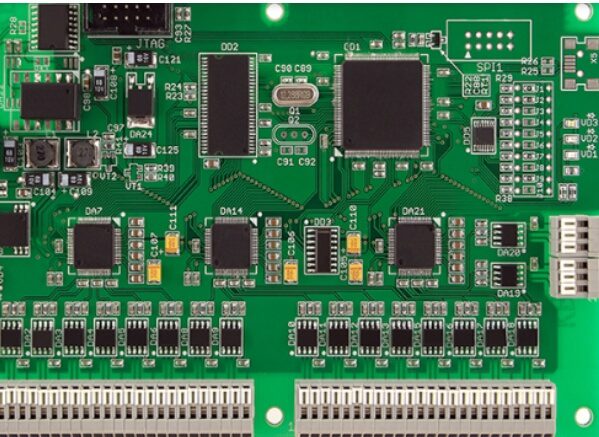
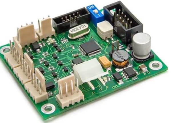
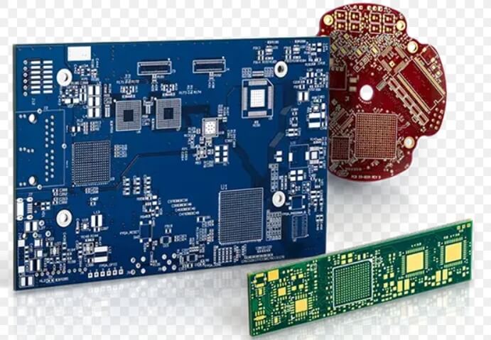
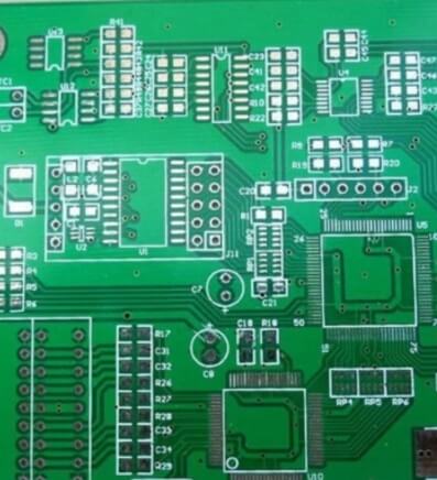
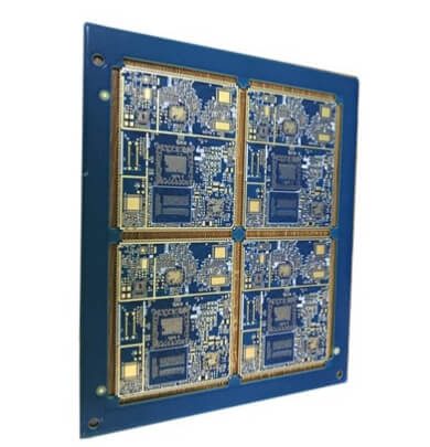
In today’s technology-driven world, the Printed Circuit Board (PCB) stands as a foundational component in electronic devices. From smartphones to complex medical equipment, PCBs are essential for ensuring reliable electrical connections and functionality. This article delves into the critical stages of PCB design, manufacturing, and final artwork, providing insights into the complexities and technicalities of creating effective circuit boards.
As electronic products become more advanced, they encounter more sources of electromagnetic interference (EMI) that can disrupt device function and potentially harm health. This guide explores strategies for designing PCB boards with optimized electromagnetic compatibility (EMC), focusing on reducing interference and increasing product resilience.
Electrostatic Discharge (ESD) can damage sensitive components such as MOSFETs, CMOS gates, and PN junctions, leading to issues like gate damage, short circuits, and even melted wiring. This guide offers practical strategies to design PCBs that effectively prevent ESD from harming the circuit.
Before explaining the inspection work after PCB wiring is completed, we will first introduce three special PCB routing techniques. The routing of PCB LAYOUT will be explained from three aspects: right-angle routing, differential routing, and serpentine routing
PCB design translates electrical schematics into a functional product, and its quality directly impacts production efficiency and product reliability. For beginners, mastering PCB layout can be challenging despite familiarity with design software, and common issues often arise. Here, seasoned engineers from KKPCB share their PCB layout insights to help avoid these pitfalls and inspire best practices.
Addressing signal integrity (SI) issues early in the PCB design process can streamline the design and eliminate the need for corrective termination devices later. Here, we outline critical steps to maintain signal integrity, from planning through testing.
Grounding is fundamental in electronic circuit design, influencing stability, noise immunity, and overall performance. Grounding techniques range from basic single-loop analog grounding to advanced grounding methods for complex mixed-signal designs. These techniques become increasingly critical in high-frequency or high-EMC (Electromagnetic Compatibility) environments. Here’s a comprehensive overview of grounding techniques and methods for reducing ground loops to enhance stability.
Multilayer PCB design follows principles similar to double-layer design, with added structural complexity and a focus on stable signal integrity and efficient routing. With experience in double-layer PCBs, moving to multilayer designs can be manageable.
Mastering these PCB design rules—like efficient grounding, proper trace sizing, and capacitor placement—significantly improves design quality and efficiency. By following these guidelines, you can reduce rework, save costs, and achieve more reliable, higher-quality PCB designs
In the PCB industry, the common types of copper foil are Rolled Annealed Copper (RA) and Electrodeposited Copper (ED).


