Key Takeaways
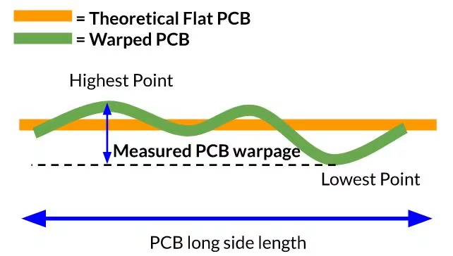
Stress during fabrication, such as thermal expansion and contraction, imbalanced copper distribution, and improper handling, can lead to warpage.
Utilize tools like feeler gauges, height gauges, contour gauges, optical profilometers, and Finite Element Method (FEM) simulations to accurately measure PCB warpage.
Effective design practices using OrCAD X, such as symmetrical component placement and proper copper distribution, combined with precise fabrication controls, can significantly reduce the risk of PCB warpage.
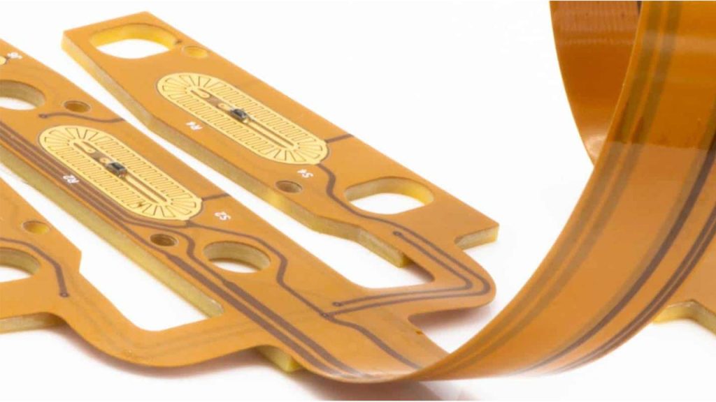
Maximize the efficiency of your design and manufacturing processes by optimizing your board development to mitigate the rigid flex PCB cost challenges
Key Takeaways
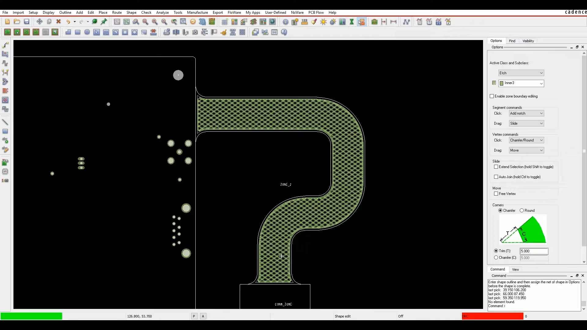
Cross-hatching significantly increases the flexibility of flex PCBs by reducing copper content.
Helps maintain optimal impedance in flex PCBs without altering dielectric thickness or signal line width.
Enables efficient manufacturing with reduced copper usage and improved resin adhesion.
OrCAD PCB Designer has the functionality to configure a 6-layer board, or any other type of PCB layer stackup to fit your exact needs
Key Takeaways
Defining two major concepts of board design and production: class and build.
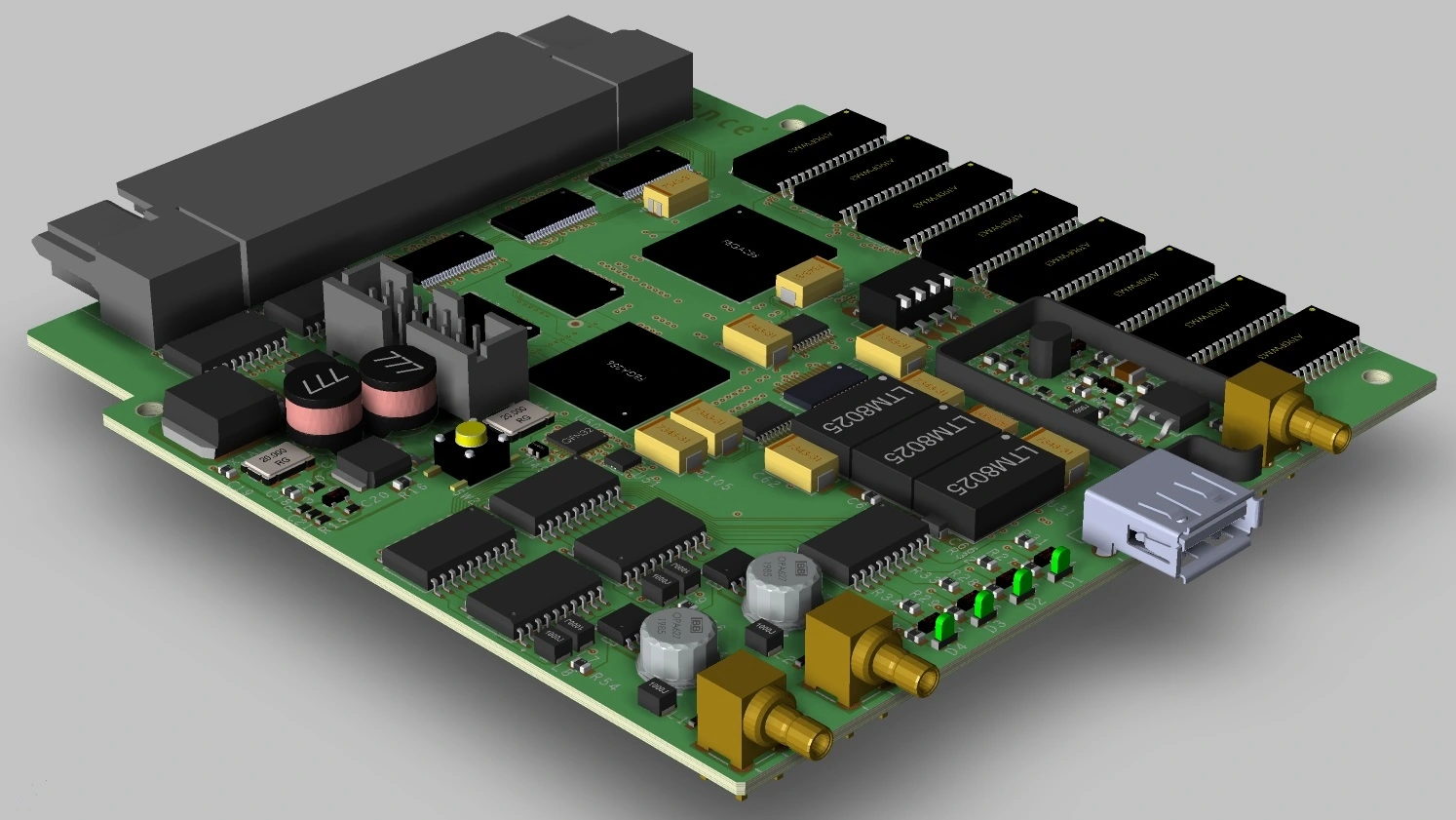
An overview of the layout department’s responsibilities: library part generation as well as placement and routing.
Stepping more granularly through each task from schematic/design document reception to manufacturing files.
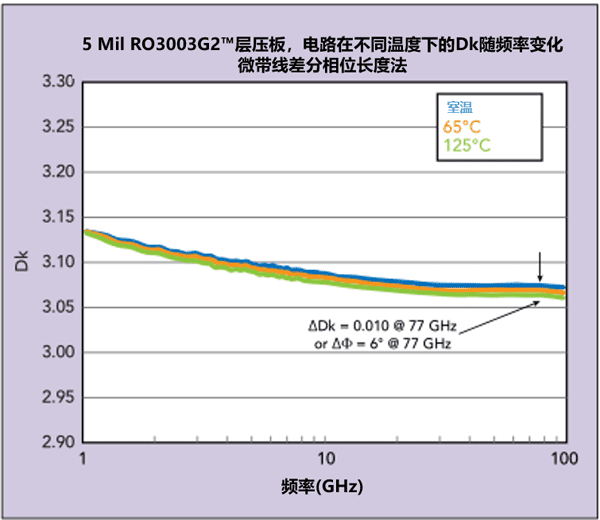
Changes in operating temperature environments are not always predictable, but they can be anticipated, especially for electronic applications that are exposed to outdoor temperatures and heat sources. Starting from the system’s circuit board, temperature effects can cause costly changes in circuit performance
Circuit pattern changes and minor anomalies are usually acceptable for low-frequency circuits, but the performance of millimeter-wave circuits is sensitive to circuit pattern changes and minor circuit anomalies
Circuit materials rely on high-quality conductors and dielectric materials to connect modern complex components to each other for optimal performance. However, these PCB copper conductors, whether DC or millimeter wave (mmWave) PCB boards, need protection against aging and oxidation
This article starts with the most basic PCB layout and discusses the role and design techniques of PCB layer stacking in controlling EMI radiation
High-frequency boards are the basis for the realization of microstrip circuit engineering. In the process of microstrip circuit design, sometimes the original design boards are out of stock, or it is necessary to use more reliable high-frequency boards for circuit design


