


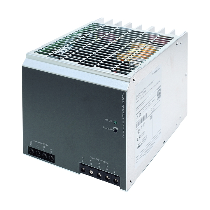
1. Background A European industrial automation customer was developing a power supply module for control systems, requiring high stability, conversion efficiency, and EMC compliance to ensure performance in demanding industrial environments. After evaluating several suppliers, the customer sought a reliable PCBA manufacturer with proven quality control and customization capabilities. 2. Application Scenario The power supply […]
1. Customer Challenge
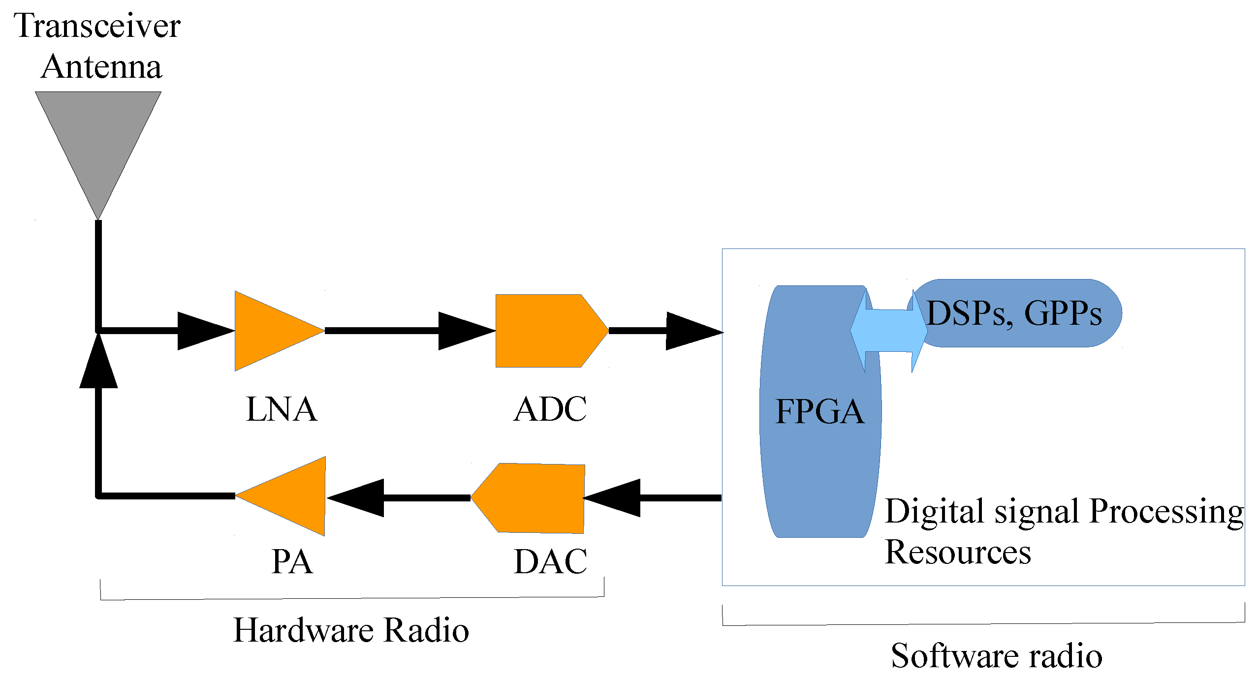
Application: Military/5G Base Station SDR Backplane
Critical Requirements:
Support 12 independent RF channels without interference
Achieve cross-channel isolation >65dB @2.4GHz
Pass FCC Part 90 certification for industrial radio equipment
Withstand harsh environments (85°C/85%RH for 1,000+ hours)
1. Customer Challenge
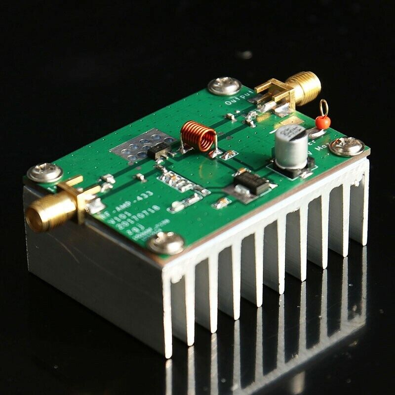
Application: 5G Base Station/Radar Power Amplifier
Pain Points:
Low Efficiency: Only 35% at 6GHz, causing excessive heat
Unstable Performance: Return loss > -15dB, signal reflection issues
Material Limitations: FR4-only PCB led to dielectric loss (Df > 0.02 @10GHz)
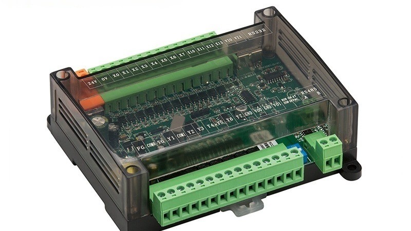
1. Background Overview Under the accelerating global trend of industrial automation, a client from Europe aimed to develop a servo drive product with high dynamic response, high-precision control, and high integration for their next-generation industrial automation equipment. After evaluating multiple suppliers, the client ultimately chose to collaborate with KKPCB, seeking a one-stop customized service from […]
1. Customer Requirements
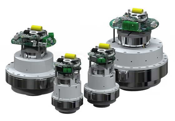
Application: Industrial robotic joint drive control
Key Challenges:
Integrate 16-channel PWM control + current sampling within 80mm × 60mm
Excessive MOSFET temperature rise (>30°C @20A), causing throttling
Compliance with IEC 61000-6-4 (Industrial EMC Standard)
1️⃣ Background Overview With the tightening of global environmental regulations and the upgrading of industrial water resource management needs, sewage treatment plants of customers in Europe, America and the Middle East are in urgent need of highly reliable and extreme environment resistant automation control systems. Traditional PLC modules have pain points such as frequent signal […]
Client: A Leading Metro System Operator (Asia)Application: Underground Tunnel Communication Systems 1. Operational Challenges Environmental Conditions: Critical Failures Observed:▶ Insulation resistance (IR) dropped to <1GΩ within 6 months▶ Bit Error Rate (BER) surged to 10⁻⁴ (vs. required 10⁻⁸)▶ Frequent corrosion-induced signal loss (3+ annual maintenance interventions) 2. KKPCB’s Robust Manufacturing Solution Core Technical Innovations Technology […]
— High-Performance Drive Control Board Empowering Industrial Control Systems 1. Background Overview A customer from the Middle Eastern region, engaged in industrial control system integration, planned to develop a two-phase open-loop stepper motor driver for use in precision mechanical control applications. The project required a control board (PCBA) with high stability, strong interference resistance, precise […]
Client Industry: European EMC Testing Equipment Manufacturer Applications: ISO 17025-Certified Probe Calibration / High-Frequency Field Measurement 1. Manufacturing Challenges Critical Requirements: Previous Supplier Limitations:▶ Manual thickness compensation caused ±8% dielectric variation▶ PTFE delamination during lamination (yield loss 15%)▶ Probe-to-probe measurement deviation >±3.5dB 2. Precision Manufacturing Innovations (A) Proprietary Process Flow Process Stage Technical Breakthrough Control Precision Material Prepreg […]
Client Industry: European Industrial Equipment ManufacturerApplications: Particle Accelerator RF Systems / Industrial Microwave Heating 1. Industry Manufacturing ChallengesCritical Requirements: Previous Supplier Issues:▶ CTE mismatch in traditional aluminum substrates caused copper layer delamination▶ Manual MOSFET soldering led to ±15% thermal resistance variation▶ Water-cooling solutions increased system complexity by 30% 2. Advanced Manufacturing Solutions (A) Core Process […]