


Best Ways to Use Skip Vias in HDI PCBs
Designing via stackups is one of the most critical aspects of HDI PCB design. Vias in HDI PCBs offer greater flexibility compared to standard boards, but they also significantly impact manufacturing costs and reliability. The choice of via style is crucial for enabling dense routing while avoiding potential failure points in the final assembly. For designs that require only a few HDI layers, skip vias are an excellent option to balance cost and reliability.
What Are Skip Vias?
Skip vias, also known as blind skip vias, are a type of blind via that skips one or more layers in the HDI stackup. Instead of terminating on the adjacent layer (e.g., Layer 2), skip vias land on a deeper layer (e.g., Layer 3 or below). They are commonly used in two types of HDI builds:
- Type 1 HDI Stackup: Standard use of skip vias to reduce cost and complexity.
- Type 3 HDI Stackup: Stackup without stacked vias, using staggered blind and buried vias.
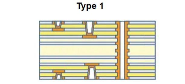
Type 1 HDI Stackup with Skip Vias
In a Type 1 HDI stackup, skip vias are used to transition from Layer 1 to Layer 3, bypassing Layer 2. This approach eliminates the need for stacked microvias, which can be prone to reliability issues during reflow cycles. By skipping Layer 2, designers can reduce manufacturing complexity and costs while maintaining signal integrity.
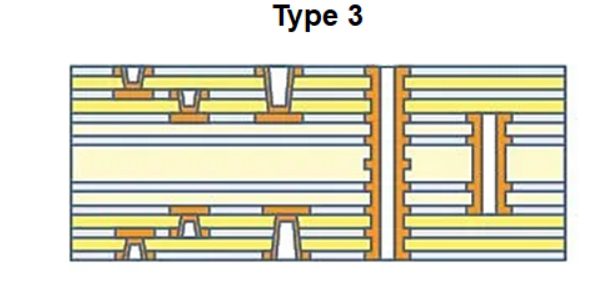
Type 3 HDI Stackup with Skip Vias
In a Type 3 HDI stackup, skip vias are used alongside blind and buried vias, but without stacking them. This staggered approach avoids the reliability challenges associated with stacked microvias. Skip vias in this configuration allow transitions from Layer 1 to Layer 3 without requiring a blind-buried via stackup.
Benefits of Using Skip Vias
- Cost Reduction: Skip vias eliminate the need for additional process steps in HDI manufacturing, such as drilling individual buildup layers. This reduces overall production costs.
- Improved Reliability: By avoiding stacked microvias, skip vias reduce the risk of via separation or breakage during reflow cycles.
- Simplified Routing: Skip vias enable efficient routing in dense designs, particularly in BGA fan-out areas, without compromising signal integrity.
How to Design Skip Vias Effectively
When designing with skip vias, it’s essential to follow specific Design for Manufacturability (DFM) rules to ensure reliability and performance:
- Aspect Ratio Limits: Skip vias must adhere to aspect ratio constraints to ensure manufacturability. This typically limits the thickness of the outer layers and the number of buildup layers (usually capped at two).
- Routing Planning: Since skip vias bypass intermediate layers (e.g., Layer 2), careful planning of routing paths is necessary. Ensure that signals requiring access to skipped layers are routed appropriately.
- BGA Fan-Out Considerations: In BGA fan-out areas, skip vias may require thinner outer layers to maintain the correct aspect ratio. Plan routing paths to avoid congestion and ensure signal integrity.
Key Design Tips for Skip Vias
- Minimize Layer Transitions: Use skip vias only when necessary to reduce complexity and cost.
- Stagger Vias: In Type 3 stackups, stagger blind and buried vias to avoid stacking and improve reliability.
- Optimize Layer Thickness: Ensure outer layers are thin enough to support the aspect ratio of skip vias.
- Leverage CAD Tools: Use advanced PCB design tools like Cadence Allegro PCB Designer to plan and optimize skip via placement and routing.
Skip vias are a powerful tool for HDI PCB designers, offering a balance between cost, complexity, and reliability. By understanding their applications in Type 1 and Type 3 HDI stackups, and following best practices for design and routing, you can create high-performance, cost-effective HDI PCBs. Whether you’re working on a simple or complex design, leveraging skip vias effectively can help you achieve your design goals while minimizing manufacturing challenges.
For advanced HDI designs, tools like Cadence Allegro PCB Designer provide the features and flexibility needed to implement skip vias and other advanced routing strategies seamlessly.