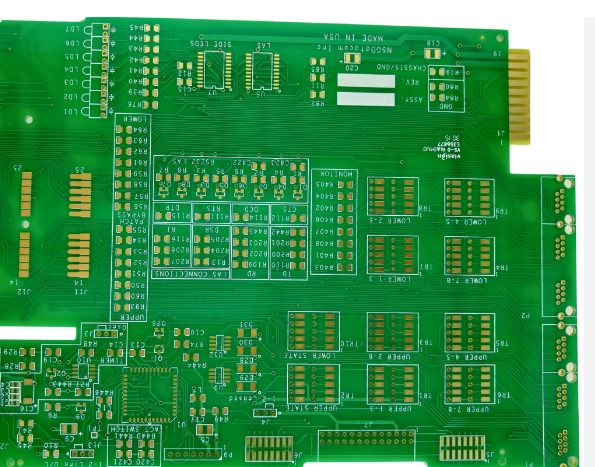
Basic Rules for PCB Layout and Wiring
I. Component Layout Rules
- Module-Based Layout:
Group related components that serve the same function into a module. Separate digital and analog circuits to minimize interference. - Clearance Around Holes:
- Non-mounting holes (e.g., positioning holes): Keep a 1.27mm clearance around them.
- Mounting holes (e.g., screw holes): Maintain 3.5mm clearance for M2.5 screws and 4mm for M3 screws.
- Avoid Vias Under Components:
Do not place vias under horizontal resistors, inductors (plug-ins), or electrolytic capacitors to prevent short circuits caused by wave soldering. - Edge Clearance:
Ensure components are at least 5mm away from the PCB edge. - Pad-to-Pad Spacing:
Maintain a spacing of at least 2mm between the outer edges of mounted component pads and adjacent plug-in components. - Metal Components:
- Keep metal-shell components (e.g., shielding boxes) isolated from other components, printed lines, and pads by at least 2mm.
- Position holes (e.g., fastener or elliptical holes) should be at least 3mm from the board edge.
- Thermal Considerations:
- Avoid placing heat-sensitive components near heating elements.
- Distribute high-heat devices evenly.

- Power Socket Placement:
- Position power sockets near the PCB edge for easy access.
- Arrange busbar terminals on the same side for streamlined cable routing and soldering.
- Ensure sufficient spacing for easy plugging/unplugging.
- Other Component Arrangements:
- Align all IC components on one side.
- Standardize the polarity marking of polar components; limit markings to two perpendicular directions.
- Copper Filling:
For areas with low routing density, fill with mesh copper foil; ensure a mesh size of 8mil (0.2mm) or larger. - Avoid Through-Holes on Pads:
Prevent solder paste leakage and cold soldering by avoiding through-holes on patch pads. Do not route critical signal lines through socket pins. - Alignment and Polarity:
- Ensure patches are aligned and character directions are consistent.
- Maintain uniform polarity marking directions for polarized devices across the PCB.
II. Wiring Rules
- Edge and Hole Clearance:
- Do not route within 1mm of the PCB edge or around mounting holes.
- Minimum Trace Width and Spacing:
- Power lines: ≥18mil.
- Signal lines: ≥12mil.
- CPU I/O lines: ≥10mil (or 8mil).
- Trace spacing: ≥10mil.
- Vias:
- Standard vias: Diameter ≥30mil.
- Component Pads and Apertures:
- DIP components: 60mil pad, 40mil aperture.
- 1/4W resistor:
- Surface mount: 51x55mil (0805).
- Through-hole: 62mil pad, 42mil aperture.
- Multilayer capacitor:
- Surface mount: 51x55mil (0805).
- Through-hole: 50mil pad, 28mil aperture.
- Routing Best Practices:
- Use radial patterns for power and ground lines.
- Avoid signal loops to maintain signal integrity.
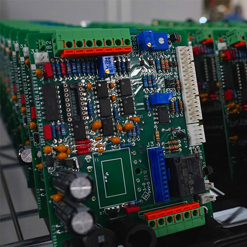
KKPCB provides global customers with one-stop services from PCB layout, prototype PCB proofing, PCB manufacturing, PCBA processing (including SMT and DIP), PCBA testing, PCBA product assembly and outbound packaging. You could provide a Gerber file or BOM list to us, we will offer the finished PCB products or PCB assembly which are satisfied with you.


