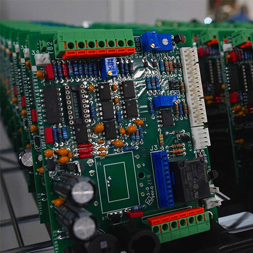
IC Substrate – Basic Introduction to Integrated Chip Substrate
What is IC Substrate?
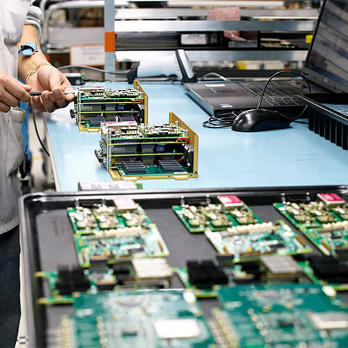
The base material of IC packages is the integrated circuit substrate (or IC package substrate). They shield the bare IC while supporting interconnection between the IC and the PCB’s trace network. As a result, the substrate has a significant impact on circuit performance. They are composed of several layers with a supporting core in the middle. In addition, the IC substrate has a network of drill holes and conductor pads. These are frequently denser than conventional PCBs. As a result, they can be quite difficult to create.
IC is an intermediate product that serves the following purposes:
- Capture a semiconductor IC chip;
- Install internal wiring to connect the chip to the PCB;
- It can protect, reinforce, and support IC chips while acting as a heat dissipation channel.
- Power and signal distribution
Some of its characteristics are:
- First, it is a single IC carrier with a board size of 150*50mm; second, its surface coating includes gold/palladium/nickel, hard gold, soft gold, Ni/Au, and so on.
- In addition to a buried blind hole, impedance, and buried resistance capacity, it has a contour tolerance of 0-50 microns.
- It has a minimum ring width of 50 microns and a pattern spacing/width of 10-80 microns.
- Fifth, its minimum aperture in the micro-hole is 0.03mm and 0.1mm in the through-hole, and its minimum PCB thickness tolerance is 0-micron.
- Finally, it has 0.1-1.5mm board thickness and 2-10 layers.
Features of an Integrated Circuit
When aligning your IC with an IC substrate, certain features in an integrated circuit must be present. IC’s characteristics include the following:
Miniaturized circuit: Because the IC is often small, the debugging, installation and design processes are usually simple and uniform.
Cost-effectiveness: Compared to other components, all ICs are relatively cheaper and perform better.
Reliability: They have fewer virtual welding and soldering joints, so integrated circuits are extremely reliable. As a result, their consistency and performance are admirable.
Lower failure rates: ICs have a lower failure rate than standard circuits.
High efficiency and energy savings: Finally, integrated circuits consume less energy, making them energy efficient.
Classification of IC Substrates
IC substrates are diverse and fall into three broad categories. The classifications are package type, o/packaging type, bonding technology, and material attributes/characteristics. We can also divide them into application fields.
Packaging type classification
The package type specifies the type of carrier. As a result, each package may necessitate a unique set of substrates.
Ball Grid Array IC substrate
This substrate is appropriate for IC packages with a high pin count (>300). We can attribute this to its superior electrical performance and heat dissipation.
Chip-scale package IC substrate
This type of substrate is thin and miniaturized. As a result, it is appropriate for smaller single-chip packages with a low pin count (CSPs). CSP IC substrate primarily uses memory, telecommunication, and electronic products with few pins.
Flip-chip IC substrate
This substrate is best suited for dominated implosion chip ties in a chip-scale flip-chip package. As a result, it has excellent heat dissipation protection against circuit failure and signal interference. FC (Flip Chip) is a chip package with low signal interference, low circuit loss, high performance, and effective thermal dissipation.
Classification by Material Characteristics
Since integrated circuits have many functions, their substrates require different material types and characteristics. The most common are:
Multi-chip module IC substrate
This IC substrate incorporates chips with various functions into a single package. As a result of its attributes, such as lightness, thinness, shortness, and miniaturization, the product may be an optimal solution. Naturally, because multiple chips packages into a single package, this type of substrate performs poorly in signal interference, thermal dissipation, good routing, and so on.
Rigid
Manufacturers make these substrates from resin. As a result, they can be made of Epoxy, Ajinomoto Build-up Film (ABF), or Bismaleimide Triazine (BT). CTE (coefficient of thermal expansion) ranges between 13 and 17ppm/°C.
Flex
This type of substrate makes with Polyimide or Polyamide resin. In addition, they both have a similar electrical performance and coefficient of thermal expansion, with CTE ranging from 13 to 27ppm / °C. ·
Ceramic
This type of substrate is made of ceramic material. It is typically made of aluminum nitride, silicon carbide, or aluminum oxide. It has a low CTE of about 6 to 8 ppm.
Classification by bonding technology
Bonding technology describes how an integrated circuit attaches to a package or external circuitry. Again, each bond may necessitate a substrate with distinct properties.
Wire bonding
The most common type of bonding is wire bonding. An operator or machine typically threads wires from the chip’s connections to the package/carrier or external circuit.
Flip Chip (FC)
Solder balls/bumps are the most common method of interconnections for facilitating the type of bonding. We flip the processor over and align it with the pads of the open circuit after placing solder balls on the chip pads. Manufacturers can make this bond using a polymer adhesive, welded joint, or solder interface.

Tape automated bonding (TAB)
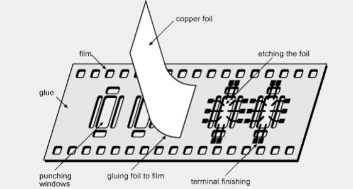
Describes the process by which bonds the manufacturers with an integrated circuit to fine conductors in a polymer-based substrate to create flexible printed circuits (FPC).
Application of Integrated Circuit Substrate PCB
We can use IC substrates for the following:
- Memory chip packaging
- Micro-electromechanical systems (MEMS) chip packaging
- Radiofrequency (RF) chip packages
- Processor chip packaging • Integrated circuitry in high-speed communication devices.
- These chips find in real-world applications such as smartphones, laptops, and tablets.
- Laptop computers, printers, and memory devices like RAM modules
- Telecommunications
- Industrial machinery and Automotive applications
- Networking applications in medical care, industrial control, aerospace, military, and telecommunications
Characteristics of an IC Substrate
Integrated Circuit substrates have a wide range of attributes and properties. Among them are the following:
- Lightweight
- IC Substrates are typically lightweight. This is primarily due to the material they employ.
- Extremely dependable
- These substrates surround the integrated circuit with a protective layer. As a result, they must be made of solid material.
- Fewer wires and solder joints are required.
- IC substrates are typically smaller than typical PCB substrates. As a result, they use fewer wires and solder joints.
- Small
- IC substrates are very small after the complete design. As a result, they require fewer materials to build.
- Durability
- IC substrates are tough, despite their small size.
What is IC Packaging?
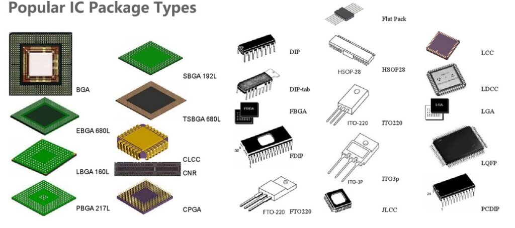
IC packaging refers to the material that houses a semiconductor device. The package is a protective casing that protects the circuit material from a corrosive environment and actual damage while also permitting electrical connectors to connect it to the mounted printed circuit board (PCB). There are many different kinds of integrated circuits. As a result, different IC packaging system designs consider, as each circuit design will have different requirements for its outer shell.
Why Is IC Packaging Necessary?
The final step in the fabrication of semiconductor devices is IC packaging. During this critical stage, the semiconductor block is encased in a package, which protects the IC from potentially harmful external elements and the corrosive effects of time. The package is simply an encasement that protects the block while promoting electrical contacts that transmit signals to an automated device’s circuit board.
IC packaging technology had advanced since the 1970s when electronics packaging manufacturers first used ball grid array (BGA) packages.
Around the turn of the century, newer packaging technologies such as the polycarbonate quad flat pack and the form-fitting outline package effectively replaced pin grid array packages.
Manufacturers like Intel used the Land Grid Array Packages Era as the decade progressed.
Meanwhile, BGAs were being phased out in favor of flip-chip ball grid arrays (FCBGAs), which had more pins than other package types. Instead of just the edges, the FCBGA includes input and output signals around the die.
IC packaging designs
IC packaging designs classify differently depending on how they comprehend the creation. Both the substrate and lead-frame types are included. The following information is available here.
- The array of pins. It uses for socketing.
- Lead-frame and dual-inline packages
- These packages imply assemblies that require pins to pass through holes.
- Package for chip scales. It’s a single-die package that can be surface-mounted directly. It has a minimum area (about 1.2 times that of a die)
- A quad-flat pack that is leadless but has a frame.
- Quad Flat with no lead but in a tiny package the size of a chip primarily used for surface mounting.
- Package with multiple chips. A multichip module, the package integrates elements, semiconductor dies, and multiple integrated circuits (ICs) onto a single substrate. As a direct consequence of this arrangement, it becomes a multichip package and feels like a larger integrated circuit.’
- Package for creating area arrays. It is a type of packaging that maximizes performance while saving space by interconnecting any remaining surface area of the chip.
Manufacturing Methods of IC Substrates
First and foremost, we must comprehend three separate PCB manufacturing processes. There are currently three types of PCB and IC substrate manufacturing processes: subtractive process (SP), additive process (AP), and modified semi-additive process (MSA) (MSAP).
Subtraction method (SP)
The most traditional PCB manufacturing process involves first plating a certain thickness of a copper layer on the copper-clad laminate, followed by a dry film to protect the circuit and through-hole, and finally etching the unnecessary copper sheet. This method’s crucial demerit is that the copper layer’s side etches during the etching process. Because of lateral etching, the minimum line width/spacing of PCB can only be greater than 50 m (2mil), limiting its use to ordinary PCB, FPC, and HDI PCB products.
The addition method (AP)
It involves first exposing the circuit to an insulating substrate containing a photosensitive catalyst, followed by selective chemical copper deposition on the exposed thick circuit to create a complete PCB. Because this method does not require lateral etching, it can achieve very high accuracy and fabrication times of less than 20 m; currently, this method has high substrate and process flow requirements, a high cost, and a low output; it comprises primarily produce WB or FC IC substrate, and its process can reach 12 M / 12 M.
MSAP (modified semi-additive process)
At first, the thin copper layer electroplates to laminate the copper-clad. The areas that do not need protection for the electroplating and the more chemical copper layer are removed by flash etching, leaving the required copper layer line. Because the copper layer is very thin at the start of electroplating, the flash corrosion time is very short, so side corrosion has little influence.
Compared to the subtraction and addition methods, the MSAP process has the advantages of high yield and low production cost, making it the most popular fine circuit board manufacturing method. This technology acknowledges commonly used in the production of CSP, WB, and FC IC substrates, as well as other fine-line substrate boards. Although the SLP (substrate-like PCB) is a printed circuit board, its minimum line width/line spacing from a process standpoint is 30 M / 30 m, so it produces by subtraction, and MSAP process technology is also required.
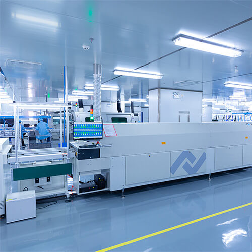
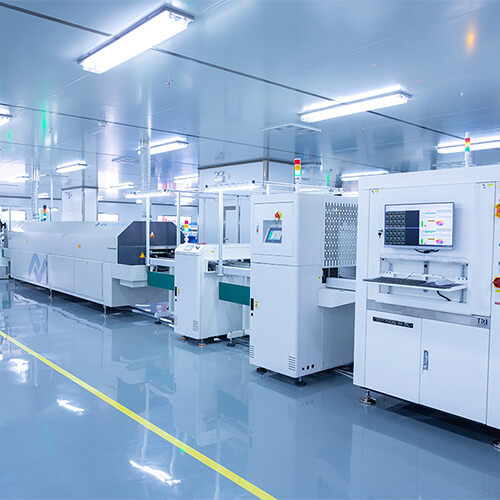
Manufacturing Process of IC Substrate PCB
Copper patterning and plating
The first step involves copper patterning and plating technology, which correlates to other aspects of diverse technology. Fine-line fabrication, uniform copper plating thickness, and circuit and control compensation technologies are part of the technology. The copper material prepares by manipulating and shaping it. As a result, this technique necessitates the use of machinery that adjusts the thickness and shape of the copper. As a result, it is the first step in the manufacturing process.
Solder mask
The second process is the solder mask, which consists of an IC substrate solder mask with solder mask printing and hole-filling technologies. Remember that the height difference between the pad and the solder mask on the substrate should be less than 15mm (ideal – 10mm and below). This helps in accomplished by applying a solder mask to the substrate. The substrate manufacturer will employ a combination of solder mask printing technology and through-hole filling equipment.
Surface treatment
This procedure entails buffing and polishing the substrate to ensure a uniform and even surface. It consists of using ENIG and ENEPIG surface finishes (the most common) to achieve a uniform thickness in the surface finish.
Reliability and inspection tests
Finally, design engineers test IC substrates for reliability and inspect their quality using specialised modern equipment. However, the process differs from that used in standard PCBs. The manufacturing company must test the last substrate for reliability and integrity during this process.
Difficulties in Manufacturing IC Substrate PCB
Compared to standard PCBs, IC substrates must overcome manufacturing challenges to implement high-performance and advanced functions.
IC Substrate Production
The IC substrate is thin and deformed properly, especially when the board is less than 0.2mm thick. To overcome the challenge, breakthroughs in board shrinking, lamination parameters, and layer positioning systems enhance the effective control of the substrate warpage and lamination thickness.
Manufacturing Technology Microvia
A conformal mask, laser-drilled micro blind vias, and copper plating are all part of microtia technology.
- Through copper openings, the Conformal Mask compensates for laser-drilled blinds via openings and blinds via apertures.
- Technological aspects are associated with Laser-Drilled Microvia fabrication: via shape, aspect ratio, side etching, left gel under via, and so on.
- Blind via Copper Plating links to the following technological factors: via filling capability, blind via openness, sinking, copper plating reliability, and so on.
Copper Plating and Patterning Technology
The following technological aspects of patterning and copper plating technology are circuitry compensation & control technology, fine line fabrication technology, and copper plating thickness uniformity control.
Finish in the Surface
Surface finish for IC substrate PCB should emphasize thickness uniformity, and ENIG/ENEPIG is fine surface finishes for IC substrate PCB.
Product Reliability Test Technology and Inspection Capability
Inspection equipment for IC substrate PCB differs from that used for traditional PCB. Furthermore, engineers capable of mastering inspection skills on special equipment must be available.
Overall, IC substrate PCB has more requirements than standard PCB, and PCB manufacturer must be equipped with advanced manufacturing capabilities and be skilled in mastering them.
Technologies Involved in Integrated Circuit Substrate
Some of the several advanced technologies in the IC production process include:
Digital Imaging Systems
It is capable of dealing with difficult ball grid array/chip scale package (BGA/CSP), flip-chip chip-scale package (FCCSP), and flip-chip ball grid array (FCBGA) applications. Aside from lowering the total cost of ownership (TCO) of the products, the process assists manufacturers/fabricators in increasing yields.
Optical Inspection Systems, Automated
Second, we have automated optical inspection systems for high-resolution, high-throughput inspection of IC substrates such as FCCSP and FCBGA. Furthermore, it employs a solo scan to capture multiple light sources while inspecting the IC substrate panel.
Systems for Ultraviolet Laser Drilling
A fine diameter of 20m, superior accuracy of 6m, and exceptional beam quality are all features of an ultraviolet laser drilling system. It also has an improved feature that supports advanced packaging applications such as low-temperature co-fired ceramic (LTCC), organic interposers, and embedded devices.
Systems for Inkjet or Additive Printing By design, the additive printing system prints dams for SiP (advanced system package), BGA, and FCCSP modules.
AOS
Automated optical shaping systems (AOS) aim to produce good short defect shaping in boards of various cutting-edge IC substrates, such as FCCSP and FCGBA. Generally, shaping fine-panel or complicated defects reduces scrap while allowing substrate manufacturers to increase yield volume.
Design Consideration for Integrated Circuits
To choose the perfect IC package or IC substrate, you should understand and examine the various technical factors of integrated circuit design. For example, you know the proper material composition and substrate for your integrated circuit package.
Understanding the difference between tape and rigid package substrate is also critical. Other companies that work well with metal conductors use laminates as substrate and lead frame substitutes.
Composition of the Material
An integrated circuit composition’s electrical, chemical, material, and electrical properties significantly impact its performance. Although laminate packages and lead frames serve different purposes, they are both made of the same material. The lead frame is the most common package format, with gold or silver wire-bond finishes connected via spot plating. It simplifies and reduces the cost of the process.
Alloy
Because it works perfectly with the core material, the alloy uses a metal frequently in porcelain packages. In contrast, plastic packaging prefers copper lead frames to safeguard the solder intersection while also providing permeability. Some countries encourage material consideration as a critical factor for SM (surface mount) plastic containers.
Lead
Due to frequent changes in European regulations, the lead finish subjection to rigorous examination regarding next-level packaging assembly. It arose from the need to find suitable replacements for tin-lead solders, which are simple to use and have become an industry standard. Fabricators, on the other hand, could not unite around one solution due to fierce rivalry. As a result, the direct question remains unresolved for some moments.
Laminates
Since the 1970s, laminates have been a viable alternative to lead frames in chip-to-board assemblies. Because of their significant cost savings over ceramic substrates, laminates are widely used in the integrated circuit packaging solutions sector. High-temperature and organic substrates continue to be the most popular laminates. These laminates are not only inexpensive, but they also have excellent electrical properties.
Applicable Substrates
Because of the popularity of semiconductor packages, there is a greater demand for appropriate interposers and substrates. A substrate is an important part of an integrated circuit package because it adds mechanical properties and allows the board to connect with external devices and components. In contrast, the interposer enables package-wide connective routing. It’s also worth noting that “interposer” and “substrate” sometimes cover interchangeably.
Conclusion
In electronics, IC substrates are crucial for trying to connect the Circuit boards and the IC chip. As a result, recognizing everything, there is to know about them can mean distinguishing between successful and flawed Circuit designs for your application store. As a result, keep the following points in mind when developing your IC for a positive experience.


