


Ball Grid Array Technology Overview
A ball grid array (BGA) is a type of surface-mount packaging that features an array of small solder balls on the underside, which serve as electrical connections to the printed circuit board (PCB). Unlike dual in-line or flat packages, ball grid arrays offer the advantage of accommodating a greater number of interconnection pins, made possible by utilizing the entire bottom surface of the device for connections instead of only relying on the perimeter.
Ball Grid Array Package Advantages
| Advantage | Description |
| Enhanced High-Speed Performance | Due to shorter connections between package leads and die connections, BGA packaging ensures improved performance at high speeds, surpassing the capabilities of perimeter-only packages. |
| High Pin Density | BGA packaging addresses the challenge of accommodating numerous pins (hundreds) in a compact integrated circuit, avoiding the quality compromise seen in densely pinned perimeter packages. |
| Superior Heat Conduction | The design of BGA packages, compared to leaded packages, offers reduced thermal resistance. This results in more efficient heat transfer from the package to the PCB, mitigating the risk of overheating. |
| Low Inductance Leads | The shortened electrical conductors in BGA packages minimize unwanted inductance, which is crucial for reducing signal distortion in high-speed electronic circuits. |
| Quality and Reliability in Soldering | BGA packages allow for a high number of pins without sacrificing the quality and reliability of solder joints, overcoming the limitations seen in traditional pin-packed packages. |
| Improved Electrical Performance | The short length of connecting conductors in BGA packages significantly lowers signal inductance, leading to enhanced electrical performance. |
| Effective Heat Dissipation | The design includes a mechanism for direct heat dissipation from the die, further reducing the risk of chip overheating and thermal damage. |
BGA Disadvantages
While BGAs have many advantages, it is worth noting some of their challenges as well.
| Disadvantage | Description |
| Lack of Compliance | BGAs lack mechanical compliance, making them susceptible to solder joint fractures due to thermal stress, flexing, and vibration. This can be addressed by matching PCB and BGA characteristics and using underfilling techniques. |
| Difficulty of Inspection | Inspecting soldering faults in BGAs is challenging once they are soldered in place. Specialized equipment like X-ray machines or electrical testing is often required. Dye and pry methods are also used for inspection. |
| Difficulties During Circuit Development | Soldering BGAs during development is impractical, and sockets are used instead. Socket types, such as those with spring pins or ZIF sockets, may be unreliable. |
| Limited Direct Access to Connections | The use of SMD BGA IC packages on the underside of the chip makes direct access to the connections challenging, rendering soldering, de-soldering, and inspection more difficult. |
Working With Ball Grid Array Packages
Ball grid array packaging technology has evolved from its predecessor, the pin grid array (PGA). In a BGA, the traditional pins found in a PGA are replaced by small pads on the underside of the package with tiny solder balls attached. The process of attaching these solder balls usually involves automated equipment, with the balls secured using a tacky flux.
When assembling a BGA device, it is carefully positioned on a PCB that has copper pads arranged in a pattern that corresponds to the location of the package’s solder balls. The board then undergoes a heating process through a reflow oven or an infrared heater, melting the solder balls.
As the solder balls liquefy, surface tension allows for the package to be perfectly aligned with the circuit board. This process also maintains the correct separation distance between the device and the PCB. As the solder cools and solidifies, it forms strong soldered connections between the BGA device and PCB, establishing the necessary electrical and mechanical bonds.
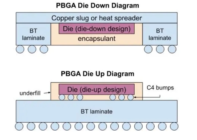
Die-Down vs. Die-Up
Die-Down Configuration
In the die-down configuration, the silicon die is attached and bonded directly to the package substrate, typically the innermost layer of the BGA package. Die-down packages are often used in thin-profile applications, such as laptops and mobile devices, where a low package height is essential. Placing the die closer to the PCB allows for better heat dissipation, as the die is in direct contact with the PCB, helping to mitigate thermal issues.
Die-Up Configuration
In the die-up configuration, the silicon die is attached to a die paddle or submount, which is then attached to the top of the BGA package. This positions the die above the package substrate. The die-up design allows for easier access to the die for testing and potential rework, which can be advantageous during the manufacturing process. “C4 bumps” refer to the specific type of solder bumps used for making electrical connections between the silicon die and the package substrate. C4 stands for “Controlled Collapse Chip Connection.”
Important Ball-Grid Array Types
There are numerous different types of ball-grid array packages, each with unique advantages.
BGA Types
| Type | Description |
| PBGA (Plastic Ball Grid Array) | Popular for double-sided PCBs, PBGA uses Bismaleimide-Triazine (BT) resin as the substrate. It ranges from 200 to 500 ball arrays, offering high reliability. |
| CBGA (Ceramic Ball Grid Array) | Known for its ceramic composition and high melting point, CBGA uses a tin-lead ratio of 10:90. It requires a Controlled Collapse Chip Connection (C4 Approach) for bridging BGAs to PCBs, offering excellent electrical performance and thermal conductivity. |
| TBGA (Tape Ball Grid Array) | Ideal for thin products requiring strong core materials, TBGA excels in heat dissipation and electrical connectivity. Depending on chip orientation, wire bond or flip-chip approaches are used. It tends to be costlier than PBGA. |
| EBGA (Enhanced Ball Grid Array) | A combination of PBGA features with additional heat sink options. It involves building a dam around chips on the substrate and sealing with liquid compounds, usually employing a wire bond approach for connectivity. |
| FC-BGA (Flip Chip Ball Grid Array) | Similar to CBGA but with a BT resin substrate. It offers shorter electrical pathways, resulting in improved electrical conductivity and performance. |
| MBGA (Metal Ball Grid Array) | Utilizing metal ceramic as the substrate, MBGA offers superior electrical performance and thermal heat dissipation. Connections are made using wire bonding, and chips are faced down. |
| Micro BGA | Micro BGA uses packaging tape substrates and elastomer between tape and chip to handle thermal expansion stress. They are small, making them suitable for high-tech, compact products. |
| Other Variants | Includes CABGA (chip array BGA), CTBGA (thin chip array BGA), CVBGA (very thin chip array BGA), DSBGA (die-size BGA), FBGA (fine BGA), FCmBGA (flip chip molded BGA), LBGA (low-profile BGA), LFBGA (low-profile fine-pitch BGA), MCM-PBGA (multi-chip module PBGA), nFBGA (New Fine BGA), SuperBGA (SBGA), TABGA (tape array BGA), TEPBGA (thermally enhanced PBGA), TFBGA (thin and fine BGA), UFBGA and UBGA (ultra fine BGA), VFBGA (very fine pitch BGA), WFBGA (very very thin profile fine pitch BGA), MAPBGA (Moulded Array Process BGA), PoP (Package on Package). |
KKPCB conducts research on special processing technologies such as ordinary double-sided boards, thick copper circuit boards, high-frequency circuit boards, HDI circuit boards, rigid-flexible circuit boards, FPC flexible boards, buried blind hole circuit boards, and IC carrier boards. Provides PCB design, PCB layout, PCB prototyping and PCB assembly services.