Ball Grid Array (BGA) Package
What is Ball Grid Array (BGA)
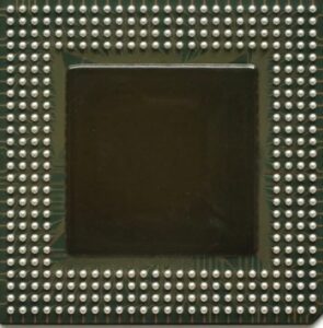
Ball Grid Array or BGA is a leadless surface mount package (SMD component). This type of surface mount package is used in surface mount technology (SMT) and utilizes an array of metal balls called solder balls for electrical interconnection. The solder balls are attached to a laminate substrate at the bottom of the package. The chip of the BGA is connected to the substrate by wire bonding or flip chip technology.
The BGA substrate has internal conductive traces for routing the chip-to-substrate bonds and connecting to the substrate-to-ball array bonds.
Ball Grid Array (BGA) Soldering
BGAs are soldered to any type of PCB using a reflow oven. When the solder balls melt in the reflow oven, the surface tension of the molten solder balls keeps the package in the correct position on the board until the solder cools and solidifies. A correct and controlled BGA soldering process and temperature are essential for good solder joints and preventing the solder balls from shorting to each other.
BGA Package Advantages
1.Ball Grid Array (BGA) has several advantages over other SMD electronic components. The most important advantage of BGA packages over integrated circuits is their high interconnect density. BGA packages also take up less space on printed circuit boards.
2. Assembling ball grid arrays onto circuit boards is more efficient and easier to manage than assembling leaded electronic components onto circuit boards because the solder required to solder the package to the circuit board comes from the solder balls themselves. These solder balls also “self-align” during the installation process
3. The lower thermal resistance between the BGA package and the PCB components is another advantage of this type of package. This allows heat to flow more freely, resulting in better heat dissipation and preventing the device from overheating.
4. BGAs also have better electrical conductivity due to the shorter path between the chip and the printed circuit board.
Disadvantages of BGA Packages
Like all other electronic packages, BGAs also have some disadvantages. Here are some of the disadvantages of BGA:
1. BGA packages are more susceptible to stress because of the bending stress of the circuit board, which can lead to potential reliability issues.
2. Once the BGA is soldered to the circuit board, it is very difficult to inspect the solder balls and solder joints for defects.
Plastic Ball Grid Array (PBGA)
A plastic BGA is a component that has a plastic molded or ball-top body. PBGA packages range in size from 7 to 50 mm with ball pitches of 1.00, 1.27, and 1.50 mm. PBGA pin counts range from 16 to 2401 pins.
The PBGA substrate is laminated and made of a glass-reinforced organic material with excellent thermal properties. Etched copper foil forms the conductive traces within the substrate. Plastic BGA assembly is typically done in “strips per substrate” where each substrate strip contains multiple package sites.
KKPCB has been providing BGA assembly, including BGA Rework and BGA Reballing services in the Printed Circuit Board Assembly industry since 2012. With state-of-the-art BGA placement equipment, high-precision BGA assembly processes, cutting-edge X-Ray Inspection equipment, and highly customizable Complete PCB Assembly solutions, you can rely on us to build high quality and high yield BGA boards.


