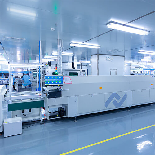
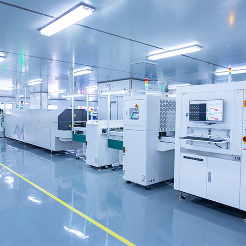
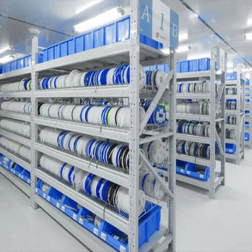
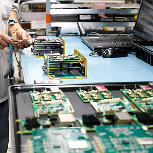
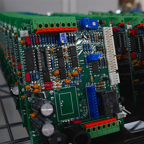
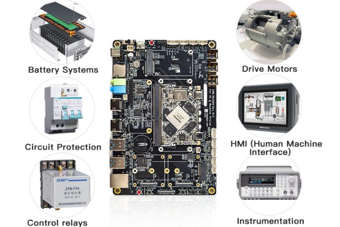
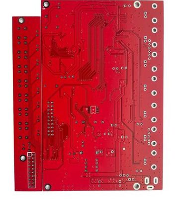
Among our other products, we specialize in providing industrial PCB assemblies that require high reliability and precision. Since electronic devices used in industrial applications need to be very stable and suitable for use in harsh conditions, industrial printed circuit boards also need to follow strict standards to thrive in industrial environments.
Special process flow for PCB processing of circuit boards As a practitioner in the PCB industry, for PCB copying, PCB design-related processes must be mastered.
As a PCB designer or manufacturer, you are constantly challenged with how to achieve better results. You want to provide new solutions or breakthroughs to problems. In some cases, these problems may require new features. It can also be a choice between module-based or custom PCB design. In any of these cases, you need a special PCB type. The growing demand for electronic functions such as high speed or high power in odd spaces makes special circuit board types essential.
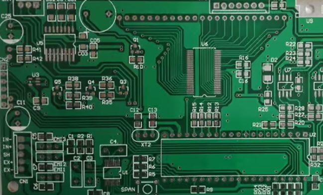
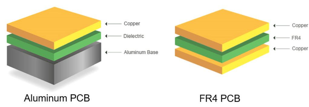
he FR4 PCBs are composed of woven fiber glass and epoxy resin with copper foil on one side. FR is the short form of Flame Retardant, a halogenated material used as a non-conducive layer with strong adherence to copper. They serve as a self-extinguisher laminating layer.
Aluminum PCB and FR4 PCB (Glass Fiber Reinforced Epoxy Resin PCB) are two common types of PCBs with significant differences in terms of materials, performance, and applications. Copper-based PCBs have better thermal conductivity than aluminum-based PCBs.
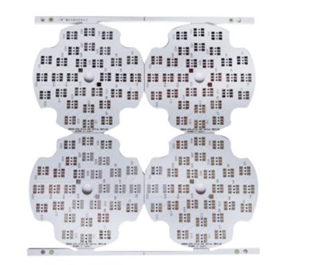
The layout of an aluminum PCB is similar to other PCBs. It has one or more layers of copper, solder mask, and silkscreen on it. However, instead of fiberglass or plastic substrates, aluminum circuit boards have metal substrates.
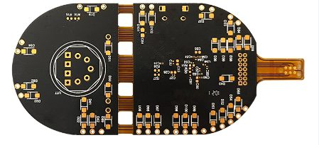
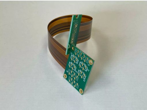
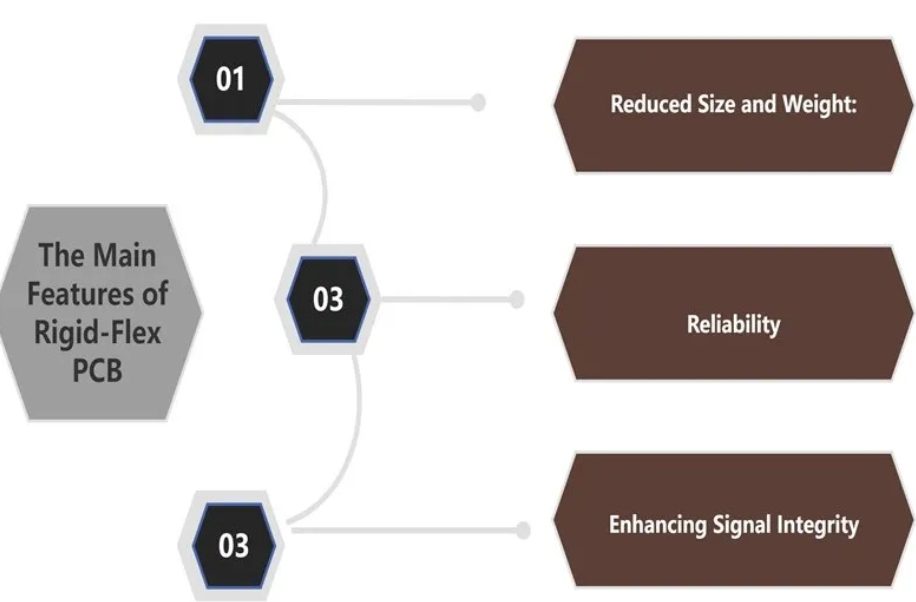
A Rigid-Flex PCB is a hybrid circuit board combining elements of both flexible circuit boards and rigid circuit boards, with an end result of a board that is able to be folded or continuously flexed and is normally formed into a flexed shape or curve during the manufacturing process.
As the name suggests, PCBs that offer strength and flexibility at the same time are Rigid-Flex PCBs. These are a hybrid design that incorporates rigid characteristics and flexible PCB characteristics
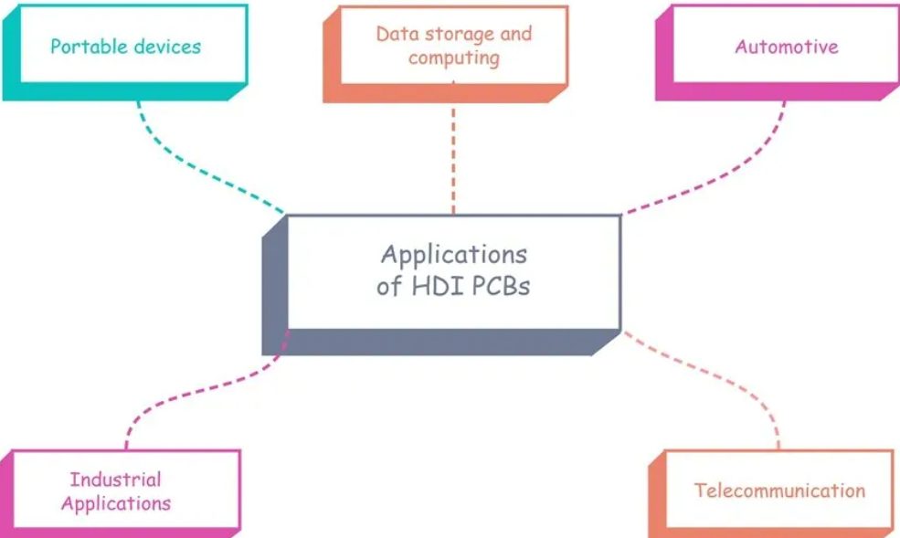
In the present world, especially in the current technological era, devices are becoming more compact and advanced. For implementing the compact and at the same time advanced electronic technology in the world, HDI PCBs contribute abundantly
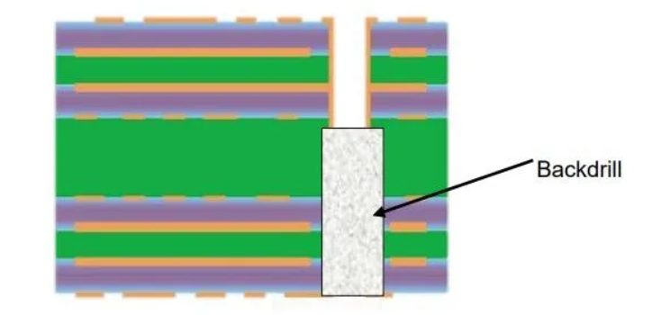
Back drilling is a method to remove the via stub from the specific layer of multilayer PCB. Via stub is a non-functional portion of a plated through hole or via barrel which can cause unwanted reflection leading to signal distortion and lower performance. It is recommended that the diameter of the back drill hole be greater than that of the via hole size.

