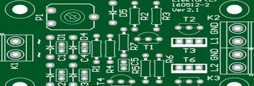
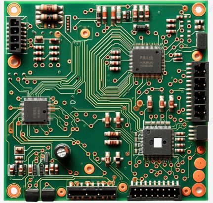
In the fast-paced world of technology, printed circuit boards (PCBs) quietly protect the functionality of electronic devices. In addition to connecting components, PCB assembly is also critical to protecting against potential threats.
Printed circuit boards (PCBs) are essential components in aerospace technology, playing a critical role in aircraft, satellites, and spacecraft. PCB assembly in aerospace requires high reliability, durability, and strict adherence to safety standards due to the extreme environmental and operating conditions encountered by aerospace systems.
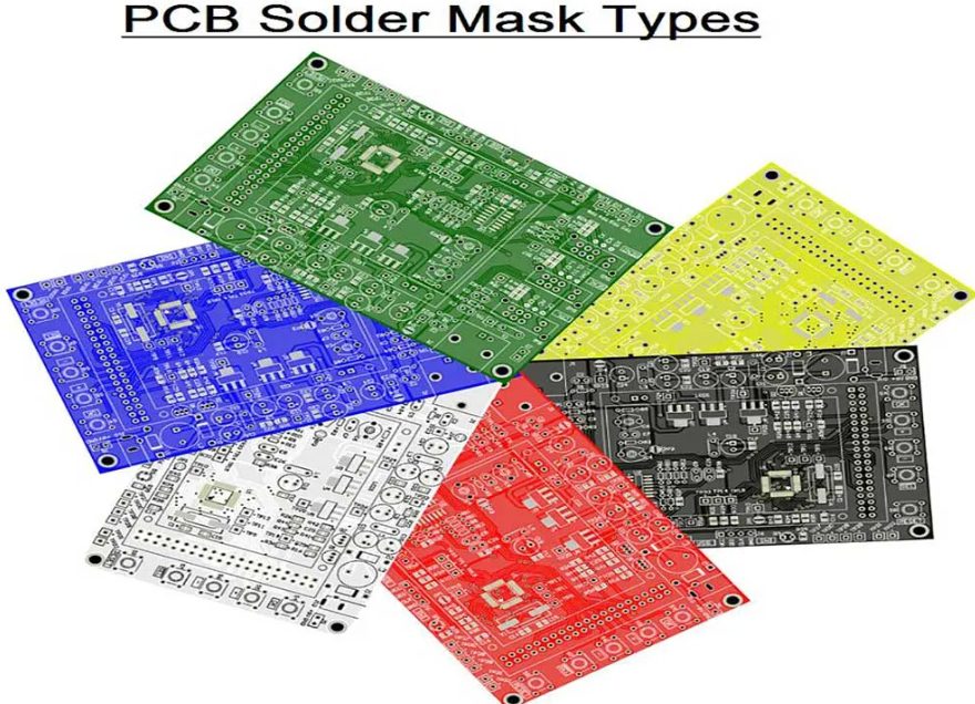
PCB solder mask is also known as PCB solder resist or PCB solder mask. It is a thin polymer protective layer PCB layer or coating that is applied on the copper traces to avoid initiating corrosion and oxidation processes after the PCB manufacturing process.
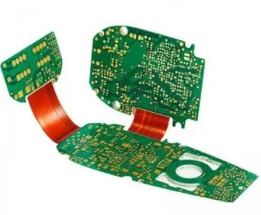
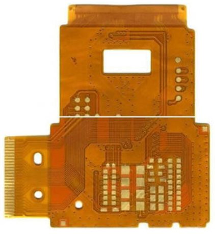
Flexible printed circuit boards (FPCBs) are essential components in modern electronic devices, offering versatility, lightweight design, and the ability to adapt to a variety of shapes. The manufacturing process of flexible PCBs involves several key steps, each of which is critical to ensuring the quality and performance of the final product.
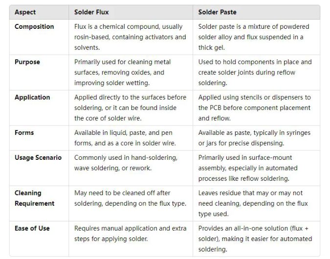
Soldering is a critical process in electronics and metalworking that is used to connect components by melting filler metal, or solder, to form reliable electrical and mechanical connections. Two key materials that assist in this process are flux and solder paste.
Automotive PCBAs help replace diesel injection pump chips, which include immobilizers and ZDCAN. People should choose automotive PCBAs correctly because they can help them keep the stock control unit in place while making simple replacements.
An industrial PCB is a circuit board designed specifically for industrial applications. It can be a PCB for a power supply system or a high-voltage motor controller. Another example is a PCB for a building’s lighting system or control electronics for automated manufacturing equipment.
PCB solder mask is one of the important components in the PCB process. In-depth knowledge of solder mask will help engineers design PCBs with better functions and quality. This article will explore the composition of PCB solder mask and its important role.
Printed Circuit Board (PCB) warpage refers to the phenomenon that the PCB plane bends or deforms due to various reasons during the manufacturing, storage or use of the PCB. This deformation may be local or overall, and is usually manifested as the PCB no longer remaining flat.
In the modern industrial system, printed circuit boards (PCBs) are the cornerstone of electronic products. From simple household appliances to complex aerospace equipment, PCBs are everywhere, assuming functions such as connection, support, and integrated circuits.


