


When designing a PCB, one of the critical decisions you’ll face is whether to use plated or unplated mounting holes. These holes are essential for securing the PCB to an enclosure or package, but the choice between plated and unplated holes depends on your design requirements, grounding needs, and mechanical considerations. Let’s explore the differences, advantages, and best practices for each type.
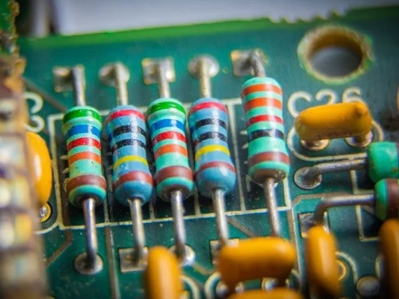
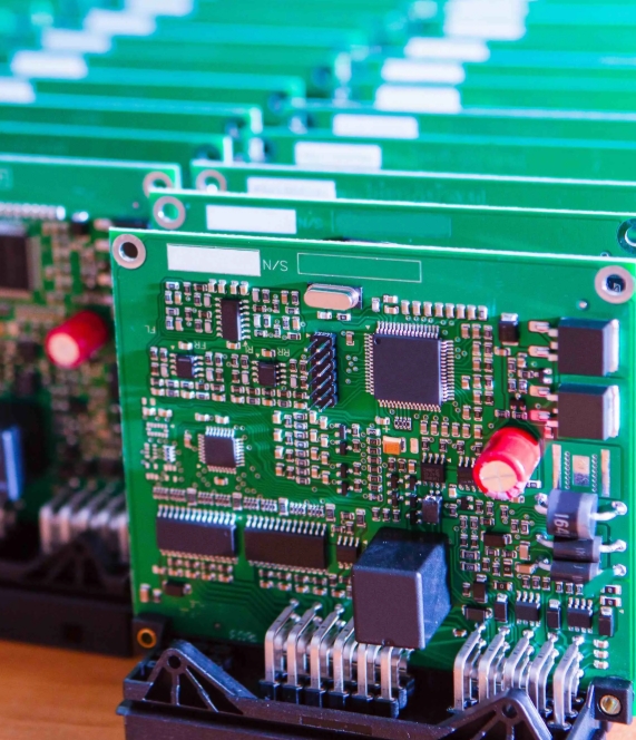
PCB resistors are designed to be mounted and soldered to printed circuit boards; they control current flow and divide voltages, among other things. PCB resistors come in many shapes and sizes, but they’re all designed to fit easily into board layouts. They have two terminals that can be soldered to the conductive traces on the PCB so they can be connected electrically to the rest of the circuit.
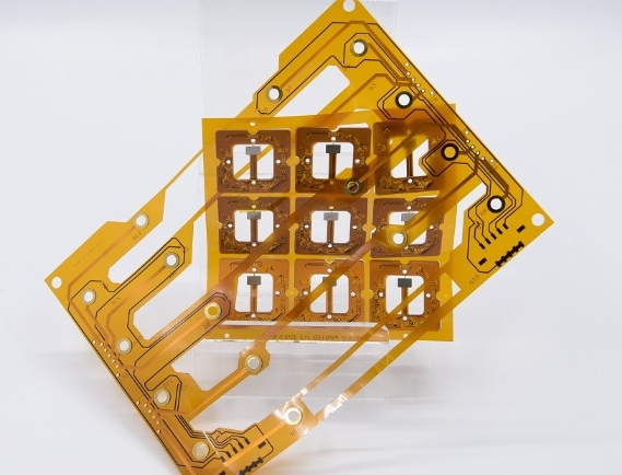
It wasn’t long ago that rigid circuit boards were the only possible electronic system method available. Whether it was entertainment or industrious, the shape of most devices was an extension of an intractable rigid board. More recently, the tide has turned: as technology has developed and matured, the enclosure is shaping the electronics inside them. Despite additional manufacturing challenges, flexible PCBs (or flex printed circuits) are enticing to product designers due to a nearly unlimited range of possibilities compared to rigid board constraints.
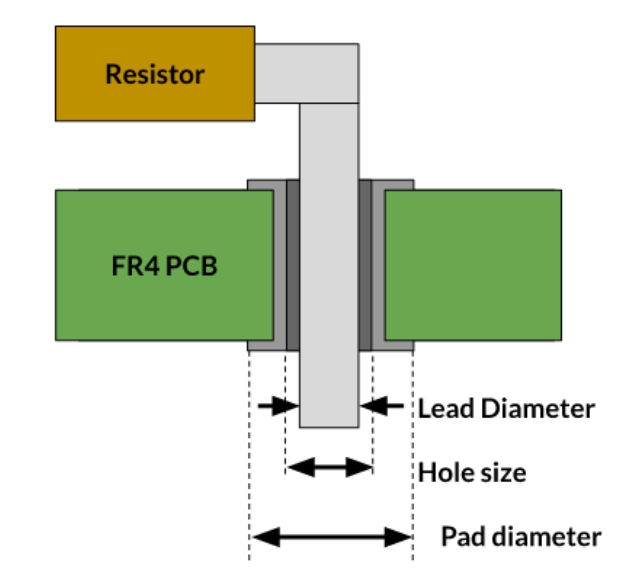
In printed circuit board (PCB) design, copper pads are points for attaching components with soldering. These pads come in two primary types: through-hole and surface-mount (SMD). Through-hole pads are designed for components with leads that are inserted through the pad’s holes and soldered on the opposite side of the board. This method ensures a mechanical and electrical bond between the component and the PCB, beneficial for long-term reliability. Read on as we discuss through-hole pad design.
PCB routing involves laying out traces to minimize interference, ensure signal integrity, and meet design requirements such as impedance control and thermal management. Traces carry electrical signals between components such as integrated circuits, resistors, and capacitors. PCB traces are usually made of copper.
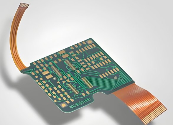
Combining the flexibility of flex circuits with the robustness of rigid boards, while leveraging High-Density Interconnect (HDI) technology, represents a significant breakthrough in modern electronics. Traditional methods like board-to-board stacking connectors or standard flex circuits often present challenges, such as cumbersome assembly and potential damage during connection. Rigid-flex PCBs offer a seamless solution, eliminating these bottlenecks and enabling more efficient designs.
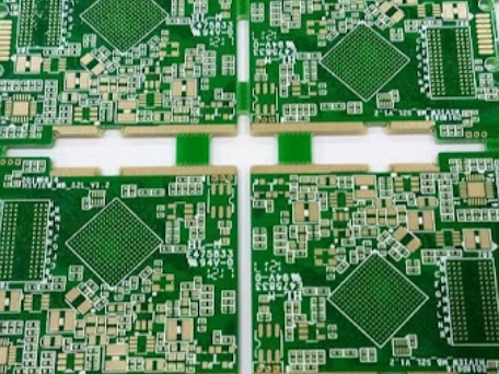
These PCB tolerances ensure that PCB circuit boards are produced precisely and can function as intended. Manufacturers adhere to specific in-house tolerance guidelines, based on international standards like IPC-A-600 Class 2, to maintain quality throughout the production process.
Electronics are becoming faster, smaller, and used in more demanding environments. Miniaturized ICs and SMDs operate at higher frequencies and require more power. Increased current demands cause voltage drops across resistive elements, generating heat and leading to temperature rises and hotspots. Over half of electronic component failures now stem from heat-related stress.
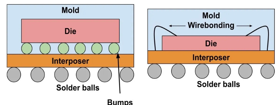
Chip-Scale Package (CSP) is a type of integrated circuit packaging technology. The size of the package is up to 1.2 times the size of the actual die, with only a single-die and a direct surface mountable package. First originating in the 1990s, it was developed as a response to the demand for smaller and more efficient packages.
Take a look at any type of multiconductor serial bus that uses single ended traces. You’ll probably see some resistors sitting around the bus being connected to driver pins and power or ground. The use of these resistors is intentional with the purpose being to set the signal level and reflection control on the bus. The other reason is placement as a pull-up resistor, where a line in the bus is pulled up to the signal power supply level.