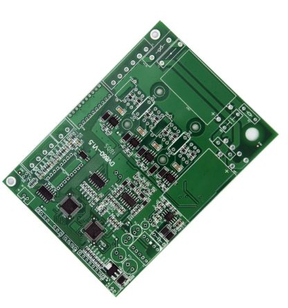
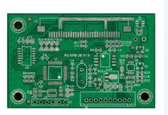
As electronic devices become increasingly miniaturized, advancements in component and wiring technologies have created new challenges for production testing. Highly integrated ICs, smaller insulation spacings, and limited access to circuit nodes have made traditional testing methods insufficient. To address these challenges, a design-for-testability (DFT) approach is essential to reduce testing costs and enhance production efficiency. This guide explores the principles, strategies, and best practices for improving PCB testability.
Understanding the classification and parameters of PCB materials is essential for selecting the right material for a specific application. Factors like flame retardancy, Tg, resin type, and base material play critical roles in the performance and reliability of PCBs.
The quality of SMT laser steel mesh depends on factors like manufacturing process, material selection, design precision, and maintenance. By adhering to best practices in cleaning, storage, and handling, you can ensure optimal stencil performance and longevity.
Achieving efficient automatic PCB wiring involves a blend of strategic planning, tool utilization, and manual refinement. By setting robust design rules, optimizing layout, and leveraging EDA tools effectively, engineers can create high-quality PCB designs that meet performance and manufacturability requirements. The iterative approach of routing, validating, and refining ensures that even the most complex designs achieve high routing rates and functionality.
RF (Radio Frequency) circuits and interfaces exhibit unique characteristics, requiring specialized design considerations. These challenges are due to the nature of RF signals and their interaction with physical elements of the circuit. Understanding these aspects ensures optimal performance in wireless communication systems. Below is an exploration of RF circuit characteristics, PCB design considerations, and optimization techniques.
Grounding is a critical aspect of PCB design, particularly in mixed-signal environments where digital and analog circuits coexist. Proper grounding ensures stable performance, minimizes noise, and improves the reliability of the overall circuit. Below are key insights and guidelines to address grounding challenges effectively.
In power supply design, PCB layout plays a critical role in ensuring the circuit’s efficiency, stability, and reliability. Below are five essential considerations for effective PCB design in power supply applications:
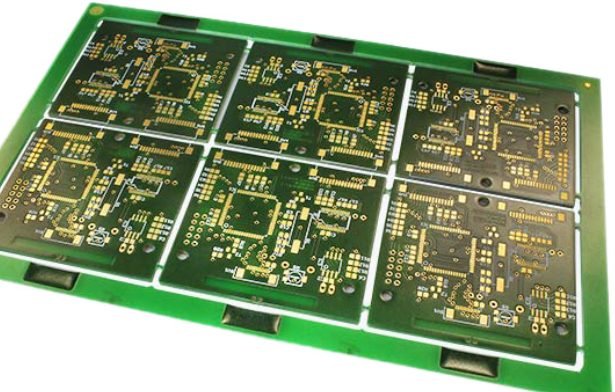
Proper packaging plays a crucial role in ensuring the safe delivery of PCBs, particularly in competitive markets where quality and presentation are key factors. Though packaging may not generate direct added value, it impacts customer satisfaction and reflects professionalism, particularly for high-precision products like PCBs.
The interconnection of electrical contacts between components and electromechanical parts in a PCB ensures the system functions as per the circuit schematic. Selecting an appropriate interconnection method depends on the specific application, balancing reliability, processability, and cost. Below are commonly used PCB interconnection methods, along with their advantages, considerations, and application scenarios
This guide delves into the four fundamental characteristics of RF circuits—RF interface, small desired signals, large interference signals, and adjacent channel interference—and highlights essential considerations for PCB design.