


As we step into 2025, the electronics manufacturing industry is poised for transformative changes driven by technological advancements, shifting consumer demands, and global economic factors. At KKPCB, we are committed to staying at the forefront of these developments to deliver cutting-edge solutions to our clients. Here’s an overview of the key trends set to reshape the industry this year.
With the continuous development of high-frequency electronic devices, especially in wireless networks and satellite communications, information products are becoming faster and higher in frequency, and communication products are moving towards large capacity and high-speed wireless transmission for voice, video, and data standardization. As a result, the next generation of products requires high-frequency substrates. The process technology for high-frequency PCB production is continuously improving to meet the diverse needs of users. Based on over ten years of experience in PCB production, this article will detail the key technical aspects and considerations for the production of high-frequency microwave PCBs.
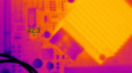
With the continuous development of electronic components, thermal management in modern electronic products has become increasingly important. Especially in highly integrated and miniaturized electronic devices, ensuring that circuit boards and components operate within the proper temperature range is a critical task for enhancing product performance and reliability. Infrared thermal imaging technology, as a non-contact temperature measurement tool, has been widely applied in the design, validation, fault diagnosis, and thermal management processes of electronic products. This article will explore the basic principles, advantages, and applications of infrared thermal imaging in the electronics industry, specifically how it helps optimize thermal management and improve product performance.
In modern electronic devices, the performance of control boards directly impacts the reliability and accuracy of the entire system. Whether in industrial automation, medical devices, or consumer electronics, data acquisition and signal processing boards (DAQ and Signal Processing PCBs) play a crucial role. To ensure that the system can efficiently and accurately process signals from sensors and other electronic components, optimizing PCB design is essential.
We explore how to optimize data acquisition and signal processing capabilities for control boards in high-precision PCB manufacturing and provide practical tips to help you achieve high-performance electronic systems.

Rogers Corporation is a leading manufacturer of advanced materials used in high-frequency PCB applications, particularly those that require excellent electrical and mechanical performance. Their copper foils are essential components in high-performance PCBs, especially in high-frequency and high-speed designs. Rogers’ copper foils are designed to maintain signal integrity and offer superior performance in applications where conventional copper may not be ideal.
The client specializes in the development and production of a wide range of microwave electronic products. These products are extensively used in satellite communication, television broadcasting, long-range communication, data and image transmission, radar, remote control, remote sensing, electronic reconnaissance, and electronic countermeasures. With deep technical expertise in microwave technology and high-frequency electronic products, the customer serves multiple high-tech industries requiring precise, reliable, and high-frequency transmission solutions.

The emergence of humanoid robots, equipped with human-like movement, perception, and intelligence, represents the next frontier of robotics. Central to this development is the advancement of printed circuit boards (PCBs) which enable the intricate control, decision-making, and sensing capabilities of these robots. This blog explores how PCB technology is powering humanoid robots and its implications for the future.
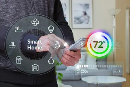
Thermostats are an essential part of our daily lives and industrial systems, regulating temperature to maintain stable conditions in both equipment and environments. However, to ensure thermostats operate reliably under various conditions, the core technology behind them—PCB (Printed Circuit Board) design—must meet high standards. This article explores the key factors to consider when designing a thermostat PCB and how to ensure its efficient and reliable performance.
In the era of smart manufacturing, industrial robots are transforming the production landscape with enhanced efficiency, precision, and safety. Central to this evolution is the indispensable role of printed circuit boards (PCBs). Acting as the “nervous system” of robots, PCBs support signal transmission, control functions, and intelligent decision-making. As robotics technology advances, so too does the design and functionality of PCBs.
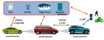
China, as the world’s largest automotive market, has positioned itself as a formidable force in the field of autonomous driving technology. With over 160 OEM manufacturers and a rapidly growing electric vehicle (EV) sector, the nation’s drive toward intelligent mobility is accelerating. This blog explores the current state of autonomous driving technology in China, highlighting key players, technological advancements, and the unique strengths that position China as a global leader in this field.