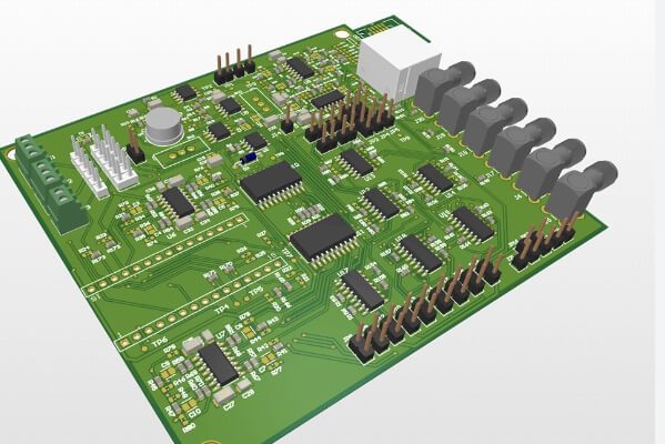
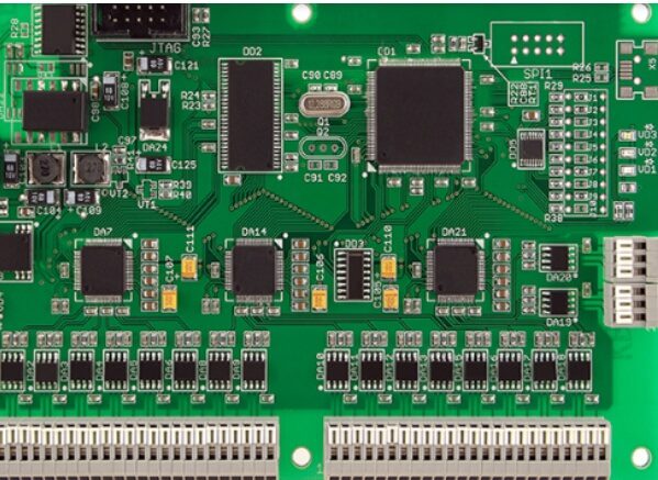
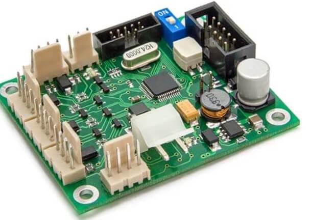
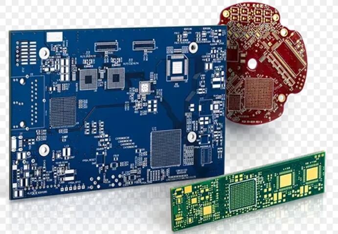
Electrostatic Discharge (ESD) can damage sensitive components such as MOSFETs, CMOS gates, and PN junctions, leading to issues like gate damage, short circuits, and even melted wiring. This guide offers practical strategies to design PCBs that effectively prevent ESD from harming the circuit.
Before explaining the inspection work after PCB wiring is completed, we will first introduce three special PCB routing techniques. The routing of PCB LAYOUT will be explained from three aspects: right-angle routing, differential routing, and serpentine routing
PCB design translates electrical schematics into a functional product, and its quality directly impacts production efficiency and product reliability. For beginners, mastering PCB layout can be challenging despite familiarity with design software, and common issues often arise. Here, seasoned engineers from KKPCB share their PCB layout insights to help avoid these pitfalls and inspire best practices.
Addressing signal integrity (SI) issues early in the PCB design process can streamline the design and eliminate the need for corrective termination devices later. Here, we outline critical steps to maintain signal integrity, from planning through testing.
Grounding is fundamental in electronic circuit design, influencing stability, noise immunity, and overall performance. Grounding techniques range from basic single-loop analog grounding to advanced grounding methods for complex mixed-signal designs. These techniques become increasingly critical in high-frequency or high-EMC (Electromagnetic Compatibility) environments. Here’s a comprehensive overview of grounding techniques and methods for reducing ground loops to enhance stability.
Multilayer PCB design follows principles similar to double-layer design, with added structural complexity and a focus on stable signal integrity and efficient routing. With experience in double-layer PCBs, moving to multilayer designs can be manageable.
Mastering these PCB design rules—like efficient grounding, proper trace sizing, and capacitor placement—significantly improves design quality and efficiency. By following these guidelines, you can reduce rework, save costs, and achieve more reliable, higher-quality PCB designs
It is generally recommended to use the method of automatic routing + manual adjustment. Automatic routing requires routing in the order of ground line – power line – clock line – others. Set the routing priority in the routing rules, 0 is the lowest level, 100 is the highest level, and there are 101 situations in total. In more complex circuit boards, considering the requirements of electrical characteristics, interference and other factors, we all use manual routing. It is forbidden to place vias on the pins of components, and the already routed lines should be locked before automatic routing. The routing should take into account both aesthetics and electrical characteristics. In particular, the routing that affects the appearance should be routed on the reverse side. In principle, do not route the front side of the product name, model and Zhongyou logo (except in special cases), and do not allow front routing between the silk screen frame and the Keepout frame (except in special cases).
HDI board is the abbreviation of High Density Inverter. It is a kind of (technology) for producing printed circuit boards. It is a circuit board with relatively high line distribution density using micro blind buried hole technology. HDI board is a compact product designed for small-capacity users. It adopts modular parallel design. One module has a capacity of 1000VA (height 1U), natural cooling, and can be directly placed in a 19″ rack. Up to 6 modules can be connected in parallel. This product adopts full digital signal process control (DSP) technology and multiple patented technologies. It has full range of load adaptability and strong short-term overload capacity, and can ignore the load power factor and peak factor.
In fact, there is no clear definition of HDI high-density manufacturing method, but generally there is a big difference between HDI and non-HDI. First of all, the aperture used in the circuit carrier made of HDI must be less than or equal to 6mil (1/1,000 inch), and the ring diameter of the hole ring must be ≦10mil, and the layout density of the line contacts must be greater than 130 points per square inch, and the line spacing of the signal line must be less than 3mil.
When discussing wiring-related technologies, two issues will be discussed: What if management cannot use a double-layer board or a ground plane, but still needs to reduce the noise in the circuit? And how to design the circuit to meet the ground plane requirements? Generally speaking, the solution is to tell management that a ground plane is necessary if reliable circuit performance is to be achieved. The main reason for using a ground plane is that the ground impedance is low and it can reduce EMI to a certain extent. But if cost constraints prevent users from achieving what they need, some suggestions provided in this article, such as star networks and correct current return paths, can also slightly reduce circuit noise.


