


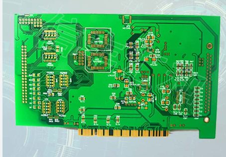
Effective anti-interference design in PCBs and MCUs involves combining hardware measures (e.g., grounding, decoupling) and software strategies (e.g., watchdogs, error-checking). By addressing interference sources, propagation paths, and sensitive devices, you can significantly enhance circuit reliability and performance.
PCB design is a delicate balance of electrical and thermal considerations, with the relationship between current and line width being a cornerstone of reliable circuit functionality. While many empirical formulas, tables, and software tools exist online to guide this aspect of design, this article consolidates the most useful references to assist engineers in optimizing PCB layouts.
Impedance plays a critical role in the functionality, reliability, and performance of printed circuit boards (PCBs). Understanding and managing impedance is essential for ensuring proper signal transmission and maintaining the integrity of the electronic devices that rely on these boards. Below is a detailed analysis of impedance and its importance in PCB design and manufacturing.
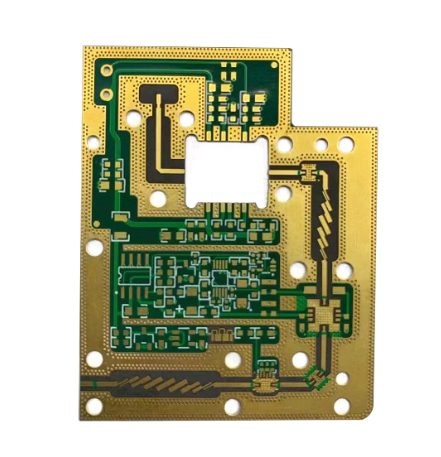
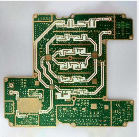
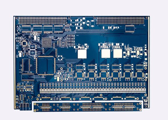
High-speed PCB design is crucial in fields like communication, computing, and graphics/image processing. Engineers in these areas often employ unique strategies tailored to their industry’s specific requirements. Below, we explore different approaches and key considerations for high-speed PCB design.
When designing high-speed PCBs, understanding the core concepts is crucial for ensuring efficiency and functionality. This guide introduces key elements such as layers, vias, pads, and more to help beginners and professionals alike.
Designing high-speed, mixed-signal PCBs requires a balance of component selection, efficient energy management, and careful layout planning. By understanding and addressing challenges like noise, parasitic coupling, and transients, designers can build robust systems capable of meeting modern performance demands
Signal isolation is essential for high-speed PCB designs to ensure system reliability, safety, and performance. With advancements in capacitive barrier technology and multifunctional ICs, designers now have access to robust solutions for complex isolation challenges. Proper selection and implementation of isolation devices will enhance overall system functionality while mitigating risks associated with varying ground potentials.
With the rise of high-speed DSPs (Digital Signal Processors) and peripherals, managing Electromagnetic Interference (EMI) has become a crucial aspect of design. In the past, issues of emission and interference were broadly referred to as EMI or RFI (Radio Frequency Interference). Today, these are part of a more nuanced area: Electromagnetic Compatibility (EMC), which encompasses both emission control and system immunity.
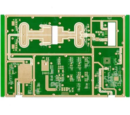
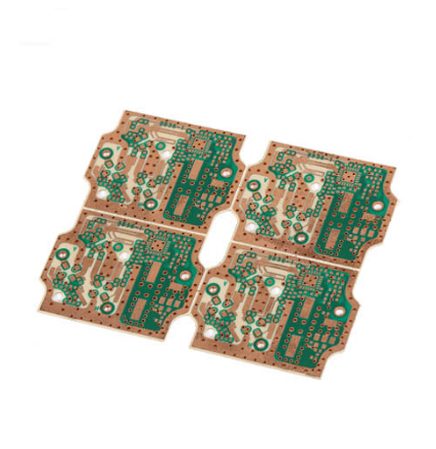
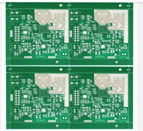
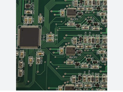
PCBs are critical in electronic devices, ensuring electrical connections between components. With increasing circuit density, proper PCB design techniques are essential to ensure reliability and reduce interference.
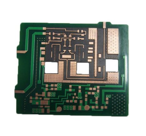
PCB interconnections can be categorized into three main types: chip-to-PCB, interconnections within the PCB, and PCB-to-external devices. High-frequency PCB designs require addressing RF effects at these interconnection points to ensure optimal performance. This guide covers techniques for minimizing RF interference, crosstalk, and return loss across these interconnection types.