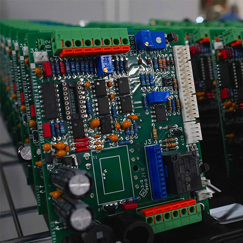
Why Choose RF or Microwave PCB Assemblies for Networking and Communication?
RF or microwave PCBs are widely recognized as the go-to solutions for networking and communication due to their superior ability to handle high frequencies. Their capacity to operate in the megahertz (MHz) to gigahertz (GHz) range makes them indispensable for modern communication applications.
The Importance of RF and
RF and microwave PCBs are designed to operate at high frequencies, enabling them to process and transmit signals effectively in wireless networks, mobile phones, satellite systems, and other communication devices. This high-frequency capability makes them essential in telecommunications, military applications, and advanced computing networks.
Applications of RF and Microwave PCBs
RF and microwave PCBs are integral to:
- Telecommunication Systems: Mobile phones, routers, and satellites.
- Military Equipment: Radars and communication systems.
- IoT Devices: Sensors and wireless modules.
- Consumer Electronics: Smart home devices and wearables.
Key Differences Between RF/Microwave PCBs and Standard PCBs
Unlike conventional analog or digital PCBs, RF or microwave PCB assemblies handle high-frequency analog signals with unique voltage and current characteristics. This distinct capability enables them to process data-intensive tasks that standard PCBs cannot manage.
Design Considerations for RF and Microwave PCB Assemblies
Developing RF or microwave PCBs requires precision and adherence to specific design standards to ensure performance and reliability. Key considerations include:
1. Noise Sensitivity
High-frequency signals are highly susceptible to noise and interference. Careful component placement and signal routing are crucial to minimize noise distortion and ensure stable performance.
2. Impedance Matching
Impedance matching is essential to reduce skin effect losses and maintain signal integrity, especially at higher frequencies.
3. Return Loss Management
Signal reflections and ringing can occur if the ground plane has discontinuities. A continuous ground plane beneath the signal paths is necessary to minimize these issues.
4. Crosstalk Prevention
Crosstalk, caused by unintended energy transfer between adjacent conductors, can be mitigated by proper spacing and routing to reduce mutual inductance and capacitance.
Materials for RF and Microwave PCBs
Choosing the right materials is critical for the performance of RF or Microwave PCB Assemblies. High-frequency PCBs often use:
- Rogers RO Laminates
- Liquid Crystal Polymers (LCP)
- Ceramic-filled Hydrocarbons
- PTFE with Woven Glass Fibers
These materials offer advantages such as low dielectric loss, excellent thermal stability, and reduced signal attenuation.
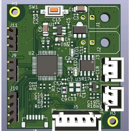
Substrate Material Selection
Substrate materials significantly impact the performance and reliability of RF and microwave PCBs. Key factors include:
- Dielectric Constant (Er): High dielectric constant materials ensure optimal signal transmission and reduced space requirements.
- Thermal Stability: Substrates must withstand varying environmental temperatures without affecting performance.
- Thickness: Proper thickness prevents bending, dielectric breakdown, and manufacturing defects.
Why RF and Microwave PCBs Are Superior
- High-Frequency Capabilities: These PCBs enable fast signal transmission with lower impedance and minimal tangent losses.
- Cost-Effective Performance: Multilayer stack-ups optimize assembly costs and enhance performance.
- Durability: Excellent temperature stability allows operation up to 40 GHz in analog applications.
- Design Flexibility: Fine-pitch components can be efficiently placed, supporting complex designs.
- Reduced Complexity: The low coefficient of thermal expansion (CTE) simplifies alignment in multilayer designs.
Final Thoughts
RF and microwave PCB assemblies are the backbone of networking and communication technologies, offering unparalleled performance for high-frequency applications. While designing these PCBs may involve complexities, careful material selection and adherence to design standards ensure optimal functionality.
Collaborating with an experienced PCB manufacturer is crucial for achieving reliable, high-quality results. Whether for telecommunications, military, or industrial use, RF and microwave PCBs remain the top choice for cutting-edge networking solutions.
KKPCB conducts research on special processing technologies such as ordinary double-sided boards, thick copper circuit boards, high-frequency circuit boards, HDI circuit boards, rigid-flexible circuit boards, FPC flexible boards, buried blind hole circuit boards, and IC carrier boards. Provides PCB design, PCB layout, PCB prototyping and PCB assembly services.

