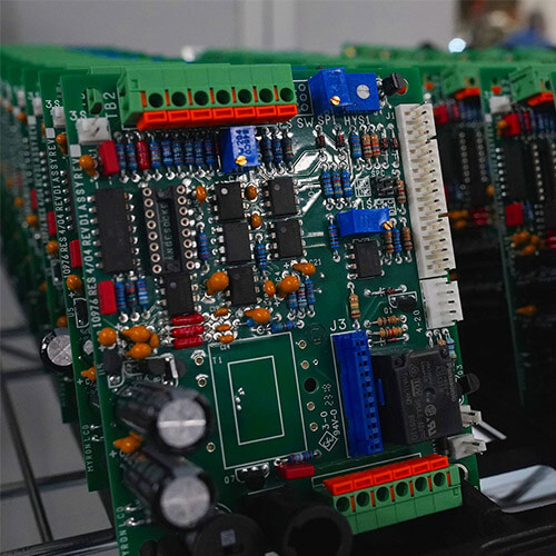
High-speed PCB design guide 6: Application technology of PowerPCB in PCB design
PCBs are critical in electronic devices, ensuring electrical connections between components. With increasing circuit density, proper PCB design techniques are essential to ensure reliability and reduce interference.
General PCB Design Principles
- Wiring Guidelines:
- Avoid Parallel Wires: Insert ground wires between input/output wires to reduce feedback.
- Conductor Width: Choose widths based on current requirements (e.g., 1.5mm width for 2A current).
- Conductor Bends: Use arcs instead of sharp angles to improve high-frequency performance.
- Copper Foil Areas: Use grid patterns for large areas to prevent warping.
- Component Layout:
- Optimize PCB size for heat dissipation and noise reduction.
- Group components by function to minimize connection lengths and mutual interference.
- Place high-frequency components and high-potential difference components apart.
- Solder Pad Design:
- Ensure pad holes are slightly larger than the device leads.
- Optimize dimensions to avoid cold soldering and ensure good electrical connections.
Anti-Interference Measures
- Power Line Design:
- Increase power line width to reduce loop resistance and align with data transmission paths.
- Grounding:
- Use single-point grounding for low-frequency circuits and multi-point grounding for high-frequency circuits.
- Separate digital and analog grounds to avoid interference.
- Ensure ground wires are thick and form closed loops to enhance noise immunity.
- Decoupling Capacitors:
- Place 10-100uF electrolytic capacitors at power inputs and 0.01uF ceramic capacitors near ICs.
- Minimize capacitor lead lengths, especially for high-frequency bypass capacitors.
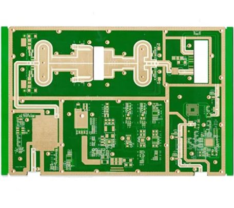
PowerPCB Design Tips
- Schematic Input:
- Use ECO mode for consistent changes between schematics and PCB layouts.
- Ensure all electrical connections are properly defined.
- Layer Selection:
- Use CAM Plane for single power/ground layers and Split/Mixed for shared layers.
- Auto Pushing:
- Enable automatic pushing for manual routing convenience, but fix pre-routed paths before auto-routing.
- Adding Positioning Holes:
- Set positioning holes to non-ECO registration to avoid unnecessary errors during checks.
- Handling SMT Devices:
- Perform fan-in and fan-out operations before routing to minimize track lengths and optimize connectivity.
- Generating Fabrication Files:
- Produce photolithography files directly in PowerPCB for easier and safer manufacturing.
Interface with ViewDraw
- Ensure seamless integration by building libraries for matching device names and maintaining consistency between schematic and PCB layouts.
Photolithography File Generation
Steps include:
- Configuring aperture settings.
- Selecting relevant layers (routing, solder mask, silk screen, drilling).
- Following precise output specifications for each file type.
KKPCB conducts research on special processing technologies such as ordinary double-sided boards, thick copper circuit boards, high-frequency circuit boards, HDI circuit boards, rigid-flexible circuit boards, FPC flexible boards, buried blind hole circuit boards, and IC carrier boards. Provides PCB design, PCB layout, PCB prototyping and PCB assembly services.

