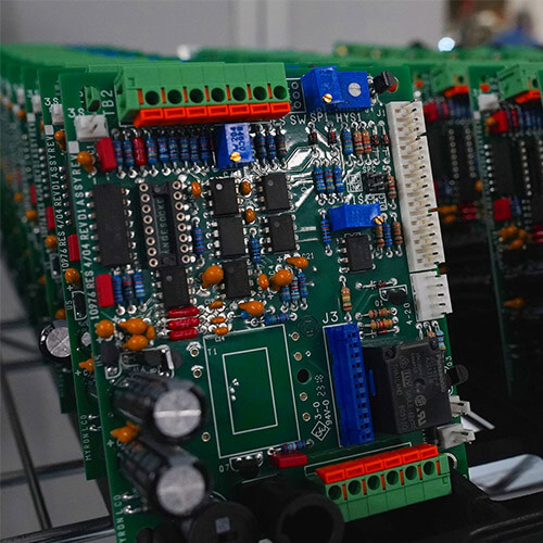
Advantages and Disadvantages of Multilayer PCBs
Multilayer PCBs (Printed Circuit Boards) are integral to modern electronics, offering unparalleled performance in compact designs. While they come with several benefits, they also present unique challenges. This article delves into the advantages and disadvantages of multilayer PCBs, providing insight into their role in electronic design and manufacturing.
Advantages of Multilayer PCBs
1. Higher Density and Efficiency
Multilayer PCBs utilize their layered structure to house a greater density of components and interconnections within limited space. This is especially beneficial for modern devices requiring complex functionality in compact designs. Shorter signal paths between components also enhance overall performance, making them ideal for high-speed applications.
2. Compact Size
The ability to stack circuits vertically minimizes the physical size of the PCB. This compactness is crucial for miniaturized devices in consumer electronics, wearables, and industrial applications, enabling smaller, lighter, and more portable products.
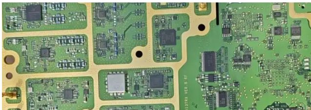
3. Improved Signal Integrity
The layered architecture allows for effective control of electromagnetic interference (EMI), crosstalk, and impedance. Ground and power planes within the stack act as shields for signal layers, ensuring stable and interference-free signal transmission—vital for high-speed and high-frequency systems.
4. Design Versatility
Multilayer PCBs support a wide range of designs, accommodating diverse electrical requirements. Layers can be dedicated to high-speed signals, power distribution, or grounding, allowing designers to create optimized layouts for specific applications.
5. Enhanced Durability and Reliability
The internal layers of multilayer PCBs are shielded from environmental factors such as moisture and dust, ensuring longevity. Their design also allows for better heat distribution, reducing the risk of overheating and related failures.
6. Better Aesthetic Appeal
Multilayer PCBs reduce the need for external wiring, resulting in sleeker, more streamlined devices. This clean design improves the overall aesthetic and enhances the user experience, particularly in consumer electronics.
Disadvantages of Multilayer PCBs
1. Increased Complexity
The design and manufacturing processes for multilayer PCBs are intricate, requiring precise alignment of layers and advanced technology. This complexity increases the likelihood of design errors and extends development timelines.
2. Higher Costs
Producing multilayer PCBs is significantly more expensive due to advanced equipment, specialized materials, and labor-intensive manufacturing. Additionally, extensive testing is necessary to ensure functionality, further driving up costs.
3. Difficulty in Repair and Modification
Fault diagnosis and repair are challenging for multilayer PCBs because inner layers are hidden. Specialized equipment is often required, and in many cases, damaged boards are not repairable, necessitating complete replacement.
4. Increased Design Time
Designing multilayer PCBs is time-consuming due to the need for meticulous planning of layer layouts, signal integrity, thermal management, and mechanical stability. Revisions to address unforeseen challenges can further extend the timeline.
5. Thermal Management Challenges
Despite better heat distribution across layers, high component density can lead to localized hotspots. Effective thermal management, such as incorporating thermal vias or heat sinks, requires careful planning and increases design complexity and cost.
Conclusion
Multilayer PCBs are indispensable for advanced electronics, offering benefits such as compactness, high reliability, and improved performance. However, their complexity, cost, and repair challenges necessitate careful planning and expertise. By balancing these advantages and disadvantages, designers can leverage the full potential of multilayer PCBs to create innovative and reliable electronic devices.
KKPCB conducts research on special processing technologies such as ordinary double-sided boards, thick copper circuit boards, high-frequency circuit boards, HDI circuit boards, rigid-flexible circuit boards, FPC flexible boards, buried blind hole circuit boards, and IC carrier boards. Provides PCB design, PCB layout, PCB prototyping and PCB assembly services.

