Advantages and Applications of Double-Sided PCB
What is a Double-Sided PCB?
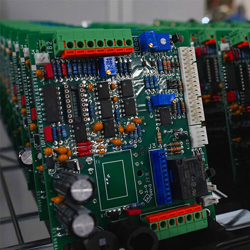
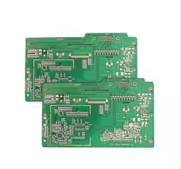
A Double-Sided PCB (also known as a Double-Layer PCB) is a type of printed circuit board where both sides of the substrate are used for placing electronic components and conductive copper traces. Unlike single-sided PCBs, which have a copper layer on only one side, double-sided PCBs feature conductive layers on both sides of the board, connected via plated-through holes (PTH), allowing circuits to connect between the top and bottom layers.
The solder mask is applied to both sides of the board, providing protection against environmental factors while ensuring proper insulation between components.
Key Characteristics of Double-Sided PCBs:
- Conductive Layers on Both Sides: Both sides of the substrate are used for conducting traces.
- Plated-Through Holes (PTH): These holes allow electrical connections between the two sides of the board.
- Surface Mount Technology (SMT): SMD components can be mounted on either side using SMT processes.
How to Make a Double-Sided PCB (DIY Process)
Creating a Double-Sided PCB at home or in a DIY setting can be relatively straightforward. Here is a step-by-step guide to help you make your own:
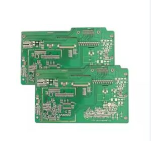
Steps to Make a Double-Sided PCB:
- Design the Layout: Use PCB design software like Proteus, Eagle, or OrCAD to create both the top and bottom layouts of the PCB.
- Print Layouts: Print both the top and bottom layouts on separate glossy paper (high-quality).
- Cut the PCB Substrate: Cut a double-sided copper-plated fiberglass PCB substrate to the required size.
- Transfer the Layouts: Using a clothing iron, transfer the top layout to the copper surface of the board by pressing it for 20-30 seconds.
- Remove Laser Ink: After transferring the top layout, use a scrubber to clean off any remaining laser ink from the PCB tracks.
- Drill Holes: Drill holes for electronic components as per the design.
- Clean the PCB: Clean the drilled side thoroughly.
- Transfer the Bottom Layout: Repeat the layout transfer process on the other side, making sure the alignment is correct.
- Etching: Place the board in a cupric chloride (CuCl₃) or ferric chloride (FeCl₃) solution for 20-30 minutes to etch the copper away, leaving behind the desired copper traces.
- Create Plated-Through Holes: Use conductive ink or a fine-tip conductive pen to make the holes conductive for proper electrical connection.
- Apply Solder Mask: Apply green solder mask on both sides of the PCB to protect the conductive traces.
- Solder Components: Once the etching and solder mask are complete, you can begin soldering the electronic components onto both sides of the PCB.
Advantages of Double-Sided PCBs
Double-Sided PCBs offer several advantages over their single-sided counterparts, including:
- Greater Flexibility: These PCBs provide more space for routing the electrical traces, which enhances design flexibility.
- Increased Circuit Density: The ability to use both sides of the board increases the overall circuit density, allowing for more compact designs.
- Reduced Board Size: By utilizing both sides, the PCB can fit more components in a smaller area, which is ideal for compact electronic devices.
- Optimized Use of Available Space: Double-sided PCBs make the best use of the board area, as components can be placed on both sides.
- Ideal for Complex Projects: The design complexity can increase, allowing engineers to create more intricate circuits.
- Cost-Effective: Double-sided PCBs offer a good balance of cost and functionality, making them a popular choice for many applications.
- Suitable for a Wide Range of Applications: These PCBs are versatile and can be used in various industries, from consumer electronics to industrial equipment.
Applications of Double-Sided PCBs
Due to their flexibility, higher circuit density, and compact nature, Double-Sided PCBs are used in a wide range of electronic devices and applications, including:
- Converters and UPS Power Systems: Providing efficient power conversion and regulation.
- Control Relays and Power Conversion: Essential in industrial control systems for switching and power regulation.
- HVAC and LED Lighting: Used in lighting systems, temperature controls, and energy-efficient applications.
- Instrumentation and Industrial Controls: Ensuring the reliable operation of industrial machinery and measuring instruments.
- Power Supplies and Regulators: Used to stabilize and regulate power in various electronic devices.
- Traffic Control Systems: Ensuring the reliable operation of traffic lights and control panels.
- Vending Machines: Powering and controlling vending machine circuits and displays.
- Line Reactors and Test Equipment: Used in test equipment to regulate voltage and in reactors for industrial purposes.
- Printers and Phone Systems: Handling power, data transmission, and control functions in devices like printers and communication systems.
- Automotive Dashboards: Enabling the complex circuits in automotive displays and control panels.
Double-Sided PCBs are an essential component in modern electronics, offering advantages such as higher circuit density, better space utilization, and cost-effectiveness. They are ideal for more complex designs and are widely used in industries ranging from consumer electronics to automotive and industrial applications.
Whether you’re designing power supplies, LED lighting, or control systems, a double-sided PCB can help optimize your design, providing flexibility and enhanced performance for a variety of applications.


