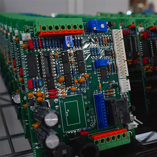
Advanced PCBs – Design, Manufacturing, and Assembly
Advanced PCBs are complex multi-layer printed circuit boards (PCBs) with significantly more layers than standard multi-layer boards. These advanced PCBs are crucial for high-end, high-precision electronic devices, which are typically found in industries like industrial equipment, instrumentation, automotive electronics, aviation, military applications, communication systems, complex computing, and space technology.
What is Required for Advanced PCBs?
The rapid advancement of technology calls for more sophisticated electronic solutions. Scientists are pushing the boundaries of space exploration with rockets, satellites, and probes aimed at the moon, Mars, and even the sun. Such ambitious projects demand complex computing systems and advanced electronic devices, which cannot be built using traditional, standard PCBs.
To meet these demanding requirements, advanced PCBs are essential in terms of materials, design, manufacturing, and assembly.
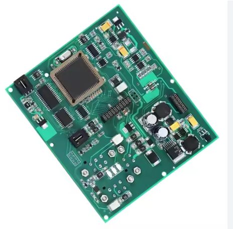
Challenges of Advanced Circuit Boards
Designing, manufacturing, and assembling advanced PCBs comes with significant challenges, and expert experience is required to ensure zero defects. These challenges include:
- High Layer Count: Advanced PCBs often have more than 40 layers, making the design and assembly more intricate.
- High Component Density: The need to fit many components within a limited space, requiring precise placement and routing.
- Routing and Constraints: Complex routing requirements to meet electrical and mechanical constraints.
- High Pin Count for BGA Packages: Handling Ball Grid Array (BGA) packages with a large number of pins requires careful routing and precision.
- Fine Pitch SMD Components: Dealing with very fine-pitch Surface-Mount Devices (SMDs), which are prone to placement and soldering challenges.
- Signal Integrity: Maintaining the integrity of high-speed signals, especially as the complexity of the design increases.
Slight mistakes in the design, selection of materials, or manufacturing processes can lead to significant failures or poor performance.
Design, Manufacturing, and Assembly of Advanced PCBs
Design Process
The PCB design process for advanced PCBs follows the same general principles as for other types of PCBs, adhering to the IPC-2221A standard for printed circuit board design. Popular design tools such as Eagle, Multisim, or even free software like Fritzing or TinyCAD are commonly used.
However, for advanced PCBs, the designer must have a deep understanding of the complex layout and constraints involved in high-layer-density designs. They need to address aspects like:
- Signal integrity management
- Thermal considerations (heat dissipation)
- Electromagnetic compatibility (EMC) requirements
Manufacturing Process
The manufacturing process for advanced PCBs follows the same basic steps as any other multi-layer PCB, but the process is more refined to accommodate the added complexity:
- Material Selection: High-quality PCB materials must be selected to ensure the desired electrical, mechanical, and thermal properties.
- Layer Construction: Each layer must be precisely aligned and laminated, requiring careful attention to detail.
- Through-Hole and Via Creation: Through-hole vias or microvias are carefully created to ensure proper interconnection between layers, without damaging sensitive circuits.
- Testing: Rigorous testing procedures are followed to ensure that the final PCB meets all performance specifications.
Assembly Process
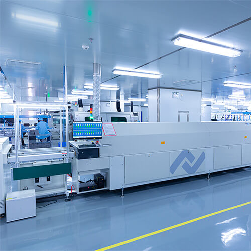
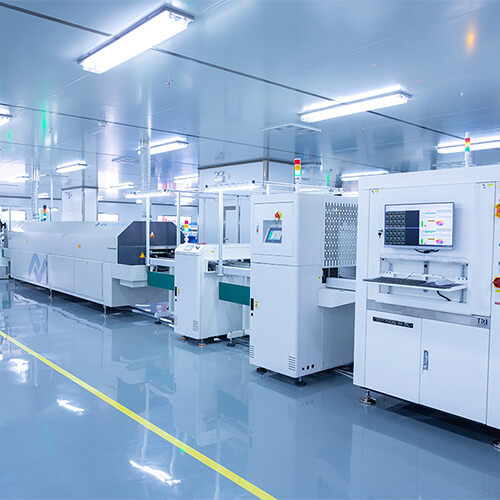
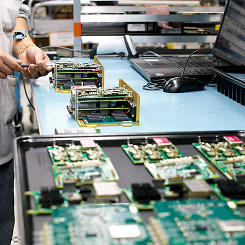
The PCB assembly process for advanced PCBs typically follows the same steps as for multi-layer PCBs, but with much greater attention to detail. Reflow soldering and wave soldering are standard methods used for component placement and soldering.
Key considerations include:
- High precision: Due to the high density of components and fine-pitch requirements, precision is crucial in placing and soldering each component.
- Automated assembly: Advanced PCBs are often assembled using automated machines to ensure speed and accuracy.
- Inspection and testing: Post-assembly inspection, often using X-ray inspection, ensures that all components are properly soldered and there are no hidden defects in the PCB.
Advanced PCBs are essential for the development of cutting-edge technologies across multiple industries. With their high layer count, dense component placement, and precision requirements, these boards are the backbone of complex, high-performance electronic systems. From design to manufacturing and assembly, every step must be carefully executed to ensure reliability and performance. As technology continues to advance, the role of advanced PCBs will only grow, driving innovation in fields ranging from space exploration to high-end consumer electronics.

