How Are PCBs Made? A Comprehensive Guide to Printed Circuit Boards
Electronic devices have transformed modern life, and at the heart of these innovations lies a critical component: the Printed Circuit Board (PCB). From smartphones and laptops to industrial machinery and household appliances, PCBs are the backbone of electronics, enabling functionality, precision, and reliability.
What Is a PCB?
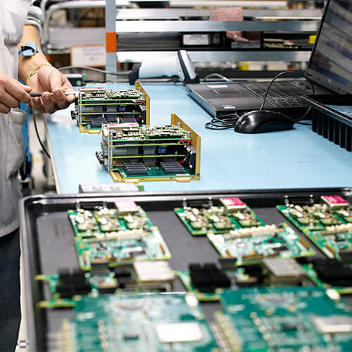
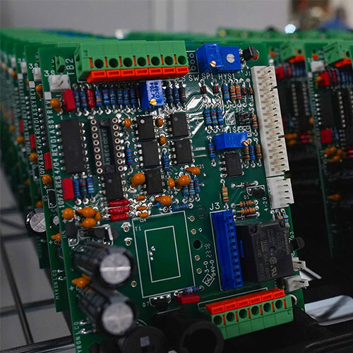
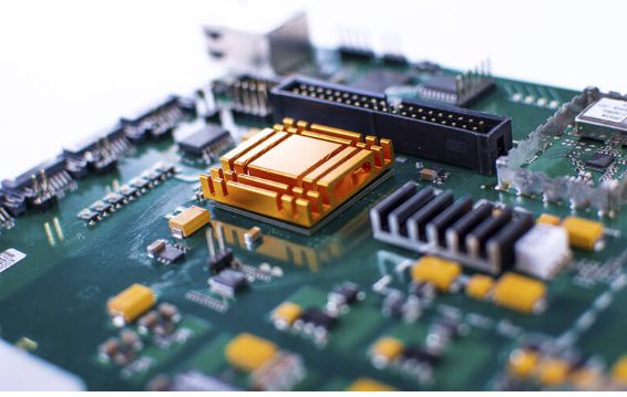
A Printed Circuit Board (PCB) is a thin board made from insulating material (substrate) with a conductive layer, typically copper, etched into patterns that connect electronic components. PCBs allow components to communicate and form complex circuits within devices.
PCBs are categorized into three primary types:
- Single-Sided Boards: Components are mounted on one side.
- Double-Sided Boards: Components are placed on both sides, connected through drilled holes.
- Multi-Layer Boards: Multiple conductive layers are separated by insulating material, enabling high-density designs for advanced applications.
Core Components of a PCB
1. Substrate
The substrate provides structural support and determines the PCB’s properties. Common materials include:
- FR-4 (glass fiber reinforced epoxy): Durable and widely used.
- Rogers RO3003: For high-frequency applications.
- Polyimides: Heat-resistant, used in high-temperature environments.
2. Prepreg
Prepreg is fiberglass cloth impregnated with resin, bonding PCB layers during lamination.
3. Copper Foil
Thin copper layers form the conductive pathways. Copper thickness varies depending on PCB design, typically between 0.5 oz (17 µm) and 3 oz (105 µm).
4. Coatings
- Solder Mask: Protects copper traces from environmental damage and oxidation.
- Silkscreen: Displays component labels and markings.
5. Vias
Vias are small holes connecting layers in multi-layer PCBs, often filled with resins for added insulation.
How Are PCBs Manufactured?
PCB manufacturing involves several detailed stages, with every step ensuring precision and quality. Below is a breakdown of the process:
Step 1: Designing the PCB
- Engineers create PCB layouts using CAD software (e.g., Gerber files).
- The design specifies copper layers, solder masks, and drill patterns.
- Prototypes are developed to ensure accuracy before production.
Step 2: Design Review
- The design is meticulously checked for errors, such as missing connections or component misalignment.
- Rigorous testing minimizes defects in the final product.
Step 3: Printing the Design
- The PCB layout is printed on a transparent film using plotter printers.
- Black ink represents conductive copper traces, while clear ink marks non-conductive areas.
Step 4: Creating Circuit Patterns
- Copper foil is coated with photoresist.
- UV light exposure hardens the circuit design areas, leaving unexposed copper removable by etching.
Step 5: Chemical Etching
- Unwanted copper is etched away using chemical solutions, leaving only the necessary traces.
Step 6: Multi-Layer PCB Processing
- Layers are bonded with prepreg under heat and pressure.
- Registration holes ensure precise alignment.
- Optical inspection verifies circuit accuracy.
Step 7: Drilling
- Holes for vias and component leads are drilled with precision guided by X-ray imaging.
- Drilled holes are plated with copper for electrical connectivity.
Step 8: Outer Layer Imaging
- A photoresist layer is applied to the outer layers, followed by UV exposure to define the circuit pattern.
- Etching removes excess copper, and tin plating protects the final pattern.
Step 9: Surface Treatment
- A solder mask is applied to prevent oxidation and improve solderability.
- Various finishes, such as HASL, ENIG, or OSP, are applied based on the design specifications.
Step 10: Quality Assurance
- Automated Optical Inspection (AOI) detects defects.
- Electrical tests check for continuity and isolation.
Step 11: Profiling and Packaging
- Individual PCBs are routed or laser-cut from the production panel.
- Boards are carefully packed to prevent damage during transportation.
Why Quality Matters in PCB Manufacturing
Every step in PCB production plays a vital role in ensuring:
- Durability: Reliable operation under various conditions.
- Precision: Alignment of layers and connections.
- Performance: Consistent functionality in electronic systems.
Conclusion
The manufacturing process of PCBs combines precision engineering, chemical processes, and rigorous quality checks to create a critical component for modern technology. Whether it’s a single-sided board for simple devices or a multi-layer PCB for advanced systems, every detail matters.
By understanding how PCBs are made, we can better appreciate the sophistication behind the electronic devices that power our world.

