A brief discussion on high-frequency PCB circuit board
With the rapid development of electronic technology and the widespread application of wireless communication technology in various fields, high frequency, high speed and high density have gradually become one of the significant development trends of modern electronic products. The high frequency and high speed digitalization of signal transmission force high-frequency PCBs to move towards micro-holes and buried/blind holes, fine wires, and uniform thin dielectric layers. High-frequency, high-speed, and high-density multi-layer PCB design technology has become an important research field.
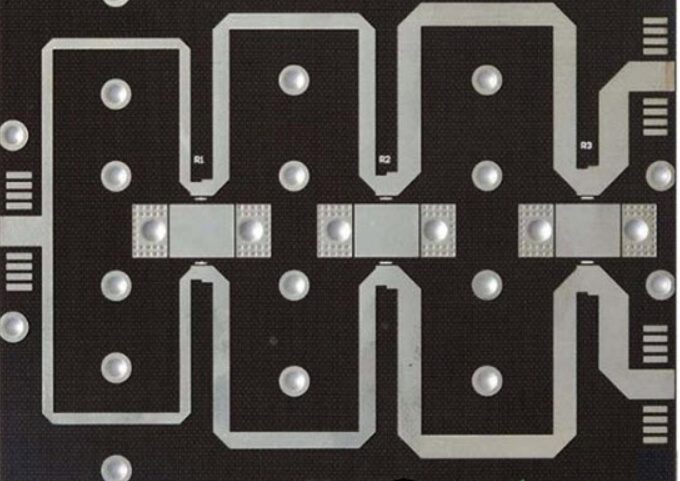
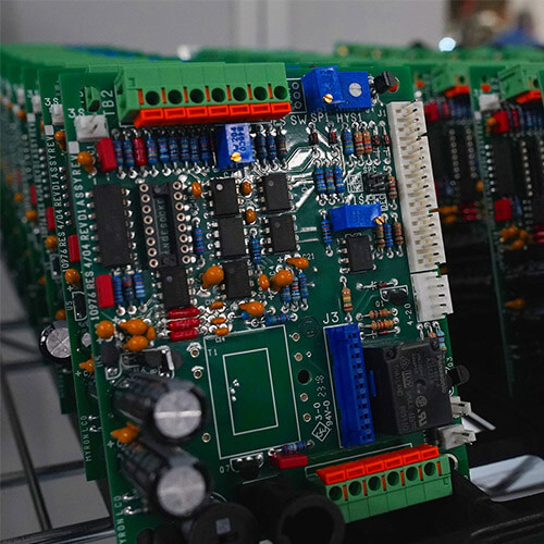
Introduction to high-frequency circuit boards: High-frequency circuit boards are special circuit boards with relatively high electromagnetic frequencies. Generally speaking, high frequency can be defined as frequencies above 1 GHz. It has very high requirements for various physical properties, precision, and technical parameters, and is often used in automotive anti-collision systems, satellite systems, radio systems, and other fields. The high-frequency circuit board provided by the utility model is provided with ribs that can block the flow of glue at the edges of the upper and lower openings of the hollow grooves of the core board. In this way, when the core board is bonded to the copper-clad boards placed on its upper and lower surfaces, the flow of glue will not enter the hollow grooves, that is, the bonding operation can be completed by one pressing. Compared with the high-frequency circuit boards in the prior art that require two pressings to complete, the high-frequency circuit board in the utility model has a simple structure, low cost, and is easy to manufacture.
High frequency PCB design High frequency circuit board wiring skills
1. The fewer bends in the leads between the pins of high-speed electronic devices, the better
It is best to use all-straight lines for the leads of high-frequency circuit wiring. If a turn is required, a 45-degree fold line or an arc turn can be used. This requirement is only used to improve the adhesion strength of the copper foil in low-frequency circuits, but in high-frequency circuits, meeting this requirement can reduce the external emission of high-frequency signals and mutual coupling.
2. The less the lead layer alternation between the pins of high-frequency circuit components, the better
The so-called “the fewer the inter-layer alternation of leads, the better” means that the fewer vias (vias) used in the component connection process, the better. A via can bring about 0.5pF of distributed capacitance. Reducing the number of vias can significantly increase speed and reduce the possibility of data errors.
3. The shorter the leads between the pins of high-frequency circuit components, the better
The radiation intensity of the signal is proportional to the length of the signal line. The longer the high-frequency signal lead is, the easier it is to couple to components close to it. Therefore, for high-frequency signal lines such as clock signals, crystal oscillators, DDR data, LVDS lines, USB lines, HDMI lines, etc., the lines are required to be as short as possible.
4. Pay attention to the “crosstalk” introduced by the close parallel routing of signal lines
When wiring high-frequency circuits, attention should be paid to the “crosstalk” introduced by the close parallel routing of signal lines. Crosstalk refers to the coupling phenomenon between signal lines that are not directly connected. Since high-frequency signals are transmitted along the transmission line in the form of electromagnetic waves, the signal line will act as an antenna, and the energy of the electromagnetic field will be emitted around the transmission line. The unwanted noise signal generated by the mutual coupling of the electromagnetic field between signals is called crosstalk. The parameters of the PCB board layer, the spacing of the signal lines, the electrical characteristics of the driving end and the receiving end, and the termination method of the signal line all have a certain impact on crosstalk. Therefore, in order to reduce the crosstalk of high-frequency signals, the following points should be achieved as much as possible during wiring:
If parallel routing in the same layer is almost unavoidable, the routing directions in two adjacent layers must be perpendicular to each other; Under the condition that the wiring space allows, inserting a ground wire or ground plane between two lines with severe crosstalk can play an isolating role and reduce crosstalk; When the space around the signal line itself has a time-varying electromagnetic field, if parallel distribution cannot be avoided, a large area of ”ground” can be arranged on the opposite side of the parallel signal line to greatly reduce interference; In digital circuits, the usual clock signals are signals with fast edge changes and large external crosstalk. Therefore, in the design, the clock line should be surrounded by a ground wire and more ground wire holes should be punched to reduce the distributed capacitance, thereby reducing crosstalk; For high-frequency signal clocks, try to use low-voltage differential clock signals and grounding methods, and pay attention to the integrity of the grounding holes; Under the premise of wiring space permitting, increase the spacing between adjacent signal lines, reduce the parallel length of the signal line, and try to make the clock line perpendicular to the key signal line instead of parallel; Do not leave the idle input terminal hanging, but ground it or connect it to the power supply (the power supply is also the ground in the high-frequency signal loop), because the hanging line may be equivalent to the transmitting antenna, and grounding can suppress the emission. Practice has shown that this method of eliminating crosstalk can sometimes be effective immediately.
5. Add high-frequency decoupling capacitors to the power pins of the integrated circuit
A high-frequency decoupling capacitor is added near the power pin of each integrated circuit block. Adding a high-frequency decoupling capacitor to the power pin can effectively suppress the interference caused by high-frequency harmonics on the power pin.
6. Isolate the ground wire of high-frequency digital signals from the ground wire of analog signals
When analog ground wires, digital ground wires, etc. are connected to the common ground wire, they should be connected with high-frequency choke beads or directly isolated and connected at a suitable location. The ground potential of the ground wire of high-frequency digital signals is generally inconsistent, and there is often a certain voltage difference between the two. Moreover, the ground wire of high-frequency digital signals often carries a very rich harmonic component of high-frequency signals. When the digital signal ground wire and the analog signal ground wire are directly connected, the harmonics of the high-frequency signal will interfere with the analog signal through ground wire coupling. Therefore, under normal circumstances, the ground wire of high-frequency digital signals and the ground wire of analog signals must be isolated. They can be connected at a suitable location with a single point, or by using high-frequency choke beads.
7. Avoid loops formed by routing
Various types of high-frequency signal routing should avoid forming loops as much as possible. If it cannot be avoided, the loop area should be as small as possible.
8. High-frequency PCB design and high-frequency circuit board wiring precautions
Reasonable selection of the number of layers: When wiring high-frequency circuit boards in high-frequency PCB design, using the middle inner plane as the power supply and ground layer can play a shielding role, effectively reduce parasitic inductance, shorten the length of signal lines, and reduce cross-interference between signals. In general, the noise of a four-layer board is 20dB lower than that of a two-layer board.
Routing method: When routing high-frequency circuit boards in high-frequency PCB design, the routing must turn at a 45° angle to reduce the emission of high-frequency signals and mutual coupling.
Trace length: When routing high-frequency circuit boards in high-frequency PCB design, the shorter the trace length, the better, and the shorter the parallel distance between the two lines, the better.
Number of vias: When routing high-frequency circuit boards in high-frequency PCB design, the fewer the number of vias, the better.
Interlayer wiring direction: When wiring high-frequency circuit boards in high-frequency PCB design, the interlayer wiring direction should be vertical, that is, the top layer is horizontal and the bottom layer is vertical, which can reduce interference between signals.
Copper foil: When routing high-frequency circuit boards in high-frequency PCB design, adding grounded copper foil can reduce interference between signals.
Ground wrapping: When wiring high-frequency circuit boards in high-frequency PCB design, ground wrapping of important signal lines can significantly improve the signal’s anti-interference ability. Of course, the interference source can also be ground wrapped to prevent it from interfering with other signals.
Signal line: When routing high-frequency circuit boards in high-frequency PCB design, signal routing cannot be looped and needs to be routed in a daisy chain manner.
Decoupling capacitor: When wiring a high-frequency circuit board in a high-frequency PCB design, a decoupling capacitor is connected across the power supply end of the integrated circuit.
High-frequency choke: When wiring the high-frequency circuit board in the high-frequency PCB design, a high-frequency choke device must be connected when the digital ground, analog ground, etc. are connected to the common ground line. Generally, it is a high-frequency ferrite bead with a wire passing through the center hole.
KKPCB conducts research on special processing technologies such as ordinary double-sided boards, thick copper circuit boards, high-frequency circuit boards, HDI circuit boards, rigid-flexible circuit boards, FPC flexible boards, buried blind hole circuit boards, and IC carrier boards. Provides PCB design, PCB layout, PCB prototyping and PCB assembly services.

