Short-term thermal effects on millimeter-wave PCBs
Electrical performance consistency is critical for producing high-volume printed circuit boards (PCBs). As PCB applications move to higher frequencies, such as fifth-generation (5G) cellular wireless networks at millimeter-wave frequencies and 77 GHz automotive radar, any inconsistencies on the PCB become very noticeable, especially when the circuits operate at shorter wavelengths of millimeter-wave frequencies. There will always be some variation in the electrical performance of PCB boards and circuit materials, so circuit designers can use computer models to explore the performance impacts of these variations. Short-term thermal effects during PCB processing can also cause performance variations. Understanding these short-term thermal effects will help enhance and improve the consistency of RF performance of PCB circuits at millimeter-wave frequencies.
Short-term thermal effects associated with PCB production are typically associated with soldering and circuit assembly, and multiple short-term thermal processes are involved in PCB processing. Generally, these thermal processes are well controlled and have little or no effect on the consistency of RF performance. It should be noted that the rework process in PCB production requires brief exposure to high temperatures, but this process is not part of the standard PCB assembly process. Although most high-frequency circuit materials will not experience performance degradation due to brief exposure to high temperatures, the characteristics and components of some circuits will experience electrical performance differences due to brief exposure to high temperatures. For example, the final surface plating of copper foil conductors may experience conductivity changes due to high temperatures.
The reflow soldering process may affect circuit material performance, but this also depends on the soldering process and materials. An important issue with short-term thermal effects on circuit materials is uncontrolled soldering processes, which are often associated with manual, hand soldering processes or rework processes. Although the short-term thermal effects of hand soldering are not considered in this article, it is important to know that processes such as hand soldering of circuit materials may affect the quality of the circuit material and the circuits made on that material.
If the temperature of the soldering iron is too high, above the cracking temperature (Td) of the circuit material, then the dielectric material near the solder joint and the high temperature will decompose. The performance degradation of the circuit material itself may not be obvious, but if the circuit is built on heat-damaged materials, then long-term reliability problems may occur. If the circuit is used for further processing on the PCB, reliability problems may also arise from some of the processing chemical components that penetrate by capillary action under the circuit conductors in the degraded area of the circuit material. In order to avoid cracking of the circuit material due to short-term thermal effects, it is important to control the soldering process temperature below the Td temperature of the circuit material and to shorten the time at the reflow soldering temperature as much as possible.
Most high-volume circuit manufacturing reflow soldering processes have well-controlled temperatures and high-temperature exposure times. These processes usually occur in multiple stages at different temperatures so that the circuit is not subjected to thermal shock due to a sharp temperature change in a short period of time. The circuit temperature is slowly raised to the reflow soldering temperature and maintained at that temperature for the shortest possible time to allow the solder to flow, and then the circuit is cooled through one or more temperature change stages. There are basic parameter settings for the reflow soldering process, but there is usually a dedicated reflow soldering process for each circuit design. The soldering area of each circuit design may have different heat dissipation effects because the circuit structure, circuit design, and components to be soldered on the PCB are different. Figure 1 shows the time-temperature relationship of a typical high-volume lead-free reflow soldering process.
Thermoplastic or thermoset materials are the most commonly used high-frequency circuit materials in the RF/microwave industry. Thermoplastic materials are softer and generally more flexible than thermoset materials. Thermoplastic materials soften when exposed to higher temperatures and melt at a certain temperature and above. Thermoset materials also soften with increasing temperatures, but do not melt. Both materials have a Td temperature, which is the temperature at which they decompose once it is reached and exceeded. Most thermoplastic materials used for RF/mmWave PCBs are based on polytetrafluoroethylene (PTFE), which has little change in performance at high temperatures and is robust when exposed to soldering temperatures.
Thermoset materials oxidize at elevated temperatures. When the temperature is below the maximum operating temperature (MOT) of the circuit, it takes a long time for the oxide to accumulate on the surface of the circuit’s dielectric material. The accumulated oxide usually increases the dielectric constant (Dk) [also known as the relative dielectric constant (εr)] and the material loss factor (Df) at the surface of the circuit material. However, depending on the temperature and material formulation, it may take months or even years for some circuits on thermoset materials to show meaningful changes in RF performance due to the oxide layer.
Typically, during short-term heat exposure caused by reflow soldering and part assembly, the temperature will be much higher than the circuit’s MOT. The MOT of RF circuits is generally 105°C, and it will take a long time (weeks, months, or years) for the oxide accumulation to affect circuit performance to become apparent based on the temperature of the MOT.
As shown in Figure 1, the reflow soldering temperature is much higher than the typical MOT value of RF circuits. The circuit materials of the PCB are exposed to reflow soldering temperatures of about 240°C during assembly. Although the exposure time to this high temperature is not long, which may usually vary from 30 seconds to 3 minutes and is considered a short-term thermal exposure, the high temperature will cause oxidation to accelerate and oxides to form more quickly. For some thermoset high-frequency laminates, the oxides formed during the reflow soldering process have little or no effect on the RF electrical properties of the circuit materials, especially when only a single reflow soldering is performed. There will be some concerns when the assembly of the PCB requires the circuit to withstand multiple reflow soldering processes and thermal exposure.
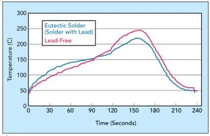
Figure 1: Example of time-temperature relationship for a high-volume reflow soldering process
Thermoset high-frequency circuit materials used in the RF PCB industry have different formulations and therefore are affected differently by the short-term heat exposure of multiple reflow soldering processes. The most commonly used reflow soldering process today is the lead-free reflow soldering process, which is more thermally aggressive than the earlier eutectic solder (lead-containing) reflow soldering process that has been replaced. Because multiple reflow soldering is required, in some designs, end users may require that multiple circuits be evaluated after the PCB has been through six lead-free reflow soldering processes. This evaluation usually requires checking the physical and mechanical integrity of the circuit assembly to ensure that the conductivity and continuity of the RF circuit channels are not destroyed during multiple reflow soldering. However, it is often overlooked whether the multiple reflow soldering processes have affected the RF performance of the circuit, resulting in changes in the performance of the PCB assembly.
For any circuit based on thermoset materials, the dielectric substrate will have some color variation after multiple lead-free reflows. Even the most oxidation-resistant thermoset high-frequency materials will have a small color variation after each lead-free reflow, as shown in Figure 2. Color variation should not be automatically associated with performance differences. Depending on the material formulation, color may or may not be related to RF performance differences.
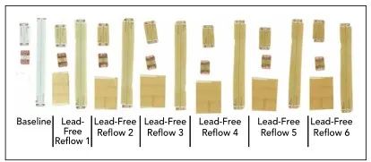
Figure 2: Circuit color on 5 mil thick RO4830™ laminate, compared after six lead-free reflow soldering cycles.
After six lead-free reflows, the color difference for a single circuit becomes apparent. In reality, the PCB and circuit components are made of a variety of high-frequency thermoset circuit materials with different colors, so the color change caused by six lead-free reflows is much smaller. Although color differences may appear subjective, they can also be more accurately measured using a colorimeter based on reflected wavelength. Figure 3 shows the color change results measured by a colorimeter for the circuit in Figure 2.
The color difference of the circuit material caused by multiple reflow soldering indicates the presence of oxide accumulation during these soldering periods. Although early oxide deposition may reduce the long-term oxide accumulation of the material and its circuit, making the long-term aging performance more consistent. As shown in the previous figures, RO4830™ material has strong oxidation resistance under high temperature exposure, so early oxide has little effect on the change of circuit material Dk.
As shown in Figure 4 for the RO4830 material, multiple lead-free reflow processes result in minimal change in the circuit material Dk performance over frequency. When the circuit was measured at mmWave frequencies after six lead-free reflow processes, the change in dielectric constant, or ΔDk, was 0.014 at 77 GHz. To further explore the impact of multiple lead-free reflow processes, Figure 5 shows the same circuits of Figures 2-4 and compares their insertion loss over frequency at mmWave frequencies. As shown in the figure, even multiple reflows at 77 GHz have a negligible effect on insertion loss performance.
The small changes in Figures 4 and 5 show that the RO4830 material exhibits robust RF performance even after six cycles of the lead-free reflow soldering process. The change in ΔDk at 77 GHz is much better than other high-frequency thermoset materials subjected to the exact same test. Other thermoset materials subjected to the same test have ΔDk values ranging from 0.013 to 0.031 due to different resin systems and formulations.
Typically, the insertion loss difference between two reflows is small and difficult to measure accurately. To better understand the difference between multiple lead-free reflows at mmWave frequencies, Figure 5 can be zoomed in around 77 GHz, as shown in Figure 6.
In Figure 6, the baseline refers to the loss measurement of the circuit under test before the lead-free reflow process. From the baseline to the first lead-free reflow (lead-free reflow 1), there is an increase in insertion loss. This is because the small amount of humidity and moisture absorbed by the circuit material during processing is expelled during the high temperature of the lead-free reflow process. The reduction of humidity or water vapor in the circuit material reduces the dielectric loss, thereby reducing the insertion loss.
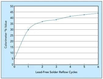
Figure 3: Colorimeter measurement results for the circuit in Figure 2.
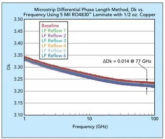
Figure 4: Dk vs. frequency after six LF reflows
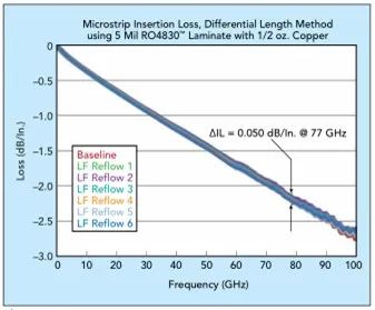
Figure 5: Insertion loss comparison after six lead-free reflow soldering cycles
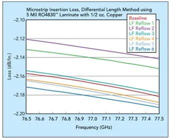
Figure 6: A zoomed-in view of the data in Figure 5 shows the impact of each lead-free reflow soldering step.
The lead-free reflow process occurs very quickly, and the insertion loss of the second lead-free reflow (lead-free reflow 2) is minimal due to the volatilization of humidity in the circuit. The short-term thermal effect of the third lead-free reflow (lead-free reflow 3) increases the insertion loss. Assuming that all moisture has been completely discharged after lead-free reflow 2, the increase in insertion loss caused by lead-free reflow 3 is entirely due to the oxidation effect. This oxidation effect will slightly increase the substrate Df, affecting the fringe field along the edge of the signal conductor. Since oxides accumulate on the exposed surface of the circuit substrate, the remaining lead-free reflow times will increase the insertion loss less.
Due to the short-term effects of high temperature exposure during the lead-free reflow soldering process, the chemical nickel-gold ENIG surface treatment will also be affected, affecting the high-frequency performance of the circuit. Surface treatments such as ENIG can provide oxidation protection for the copper foil on the circuit surface, but they will also increase conductor loss, resulting in increased circuit insertion loss. By comparing different PTFE circuits with ENIG surface treatments made by different processing board factories, it is determined that the ENIG circuit can affect the RF performance after lead-free reflow soldering, especially at lower frequencies. Figure 7 shows the typical response of the loss of the ENIG circuit after the lead-free reflow soldering process.
Figure 7: Insertion loss of an 8-inch long circuit with ENIG surface finish, comparing insertion loss before reflow and after two lead-free reflows.
The results in Figure 7 are based on a 50 Ω microstrip transmission line circuit on a 5 mil RO3003™ laminate with 0.5 oz, rolled copper from Rogers Corporation. The PTFE-based RO3003 circuit material is well known for its electrical and mechanical stability after multiple lead-free reflow soldering processes. Initially, this test was repeated using a microstrip circuit on a different PTFE laminate with similar results. Therefore, to further investigate the effects of the lead-free reflow process, this measurement analysis was repeated on a microstrip circuit on a 5 mil RO3003 laminate with an ENIG finish from a different fabricator with similar results.
Solder may also affect the electrical performance of the circuit. Therefore, in order to better understand the impact of the lead-free reflow soldering process on the circuits and materials studied in this article, no solder was added to the circuits in any of the test studies. More specifically, the circuits were subjected to the lead-free reflow process without the addition of solder, that is, only the high temperature process. In this way, the impact of the lead-free soldering process can be studied without the changes in RF performance caused by the solder.
Higher frequency
Circuits operating at millimeter-wave frequencies generally do not use ENIG surface treatment because ENIG will cause additional loss in these frequency bands. The wavelength is short and the skin depth is small in the millimeter-wave band, and the thickness of the nickel layer is thick enough in comparison. Changes in the thickness of the nickel layer will also cause changes in electrical performance at millimeter-wave frequencies. Surface treatment at millimeter-wave frequencies can use chemical tin, chemical silver, or organic solderability protection film (OSP).
Low-frequency millimeter-wave automotive radar circuits often use chemical tinning for surface treatment. Different board factories may have slightly different chemical tinning processes, and different chemical tinning has slightly different effects on the RF performance of the circuit, but they are not significant. However, chemical tinning will cause differences in the electrical performance of high-frequency circuits after lead-free reflow soldering, as shown in Figure 8.
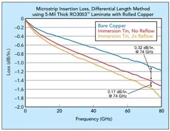
Figure 8: Insertion loss comparison of 50 Ω microstrip transmission line circuit with bare copper, tinned copper, and tinned copper circuit after two lead-free reflow solderings
Electroless silver is also widely used in automotive millimeter wave radar circuits. Several different electroless silvers were studied and found to have little effect on electrical performance. Compared to the baseline bare copper circuit, the electroless silver circuit showed almost no difference in electrical performance over a wide frequency range. Figure 9 shows the difference in insertion loss of the transmission line circuit of bare copper and electroless silver.
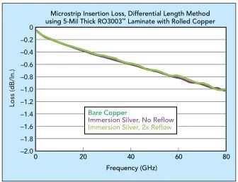
Figure 9: Insertion loss comparison of 50 Ω microstrip transmission line circuit with bare copper, silver and silver circuit after two lead-free reflow soldering
When using chemical silver finishes at higher frequencies, oxidation of the silver itself can be a concern. Over time, the surface of the immersion silver will gradually lose its luster, resulting in poor appearance. It is well known that the conductivity of most metal oxides is much lower than the metal itself. As the oxide accumulates, the conductor loss increases, so the insertion loss of the circuit will also increase. Fortunately, the conductivity of silver oxide is very close to that of silver itself, and even if the silver oxide accumulates further and loses its luster and causes poor appearance, it will not significantly change the RF performance of the immersion silver circuit. Verification has found that this result remains valid for at least 4-5.
in conclusion
Circuit materials need to go through a number of different processes to build a PCB circuit, many of which expose the materials to high temperatures at different times. If a circuit needs to undergo multiple lead-free reflow soldering processes, it will be repeatedly exposed to high temperatures, which may cause differences in electrical performance even though the time is short. Therefore, for materials used in RF/millimeter wave circuits, the first consideration is to obtain the best electrical performance at high frequencies, and the short-term thermal effects of the materials during the assembly and soldering process cannot be ignored.


