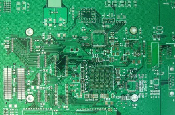
HDI Board: High Density Interconnect Technology
HDI boards, or High Density Interconnect boards, represent a significant advancement in PCB manufacturing, particularly suited for high-density circuit applications. These boards utilize micro-blind buried via technology to achieve compact designs with high line distribution density. Key characteristics include:

- Manufacturing Process: HDI boards typically employ micro-blind buried via technology, necessitating non-mechanical drilling methods such as laser drilling due to the smaller feature sizes. This technology supports higher circuit density with finer line spacing and micro-vias less than 150 microns in diameter.
- Process Variants: HDI boards are classified based on the number of build-up layers:
- First-order: 1+N+1
- Second-order: 2+N+2
- Third-order: 3+N+3
- Fourth-order: 4+N+4
- Applications: Widely used in mobile phones, digital cameras, laptops, automotive electronics, and other compact digital products, HDI boards enhance miniaturization while meeting stringent performance standards. They are essential for 3G mobile phones, IC substrates, and advanced digital devices.
- Advantages:
- Reduced PCB costs compared to traditional lamination processes for eight or more layers.
- Increased line density and improved electrical performance.
- Enhanced reliability, thermal properties, and resistance to electromagnetic interference.
- Enables advanced assembly technologies like BGA and CSP.
- Market Trends: The demand for HDI boards is driven by the rapid growth in mobile phone production. Asia, particularly China, dominates HDI board manufacturing, catering to global demand. Future growth is expected with advancements in mobile technology and electronic miniaturization.
- Production Challenges: Challenges include precise alignment for fine pitch components, maintaining high yield rates, and optimizing imaging processes to reduce defects and material costs.
In summary, HDI boards represent the forefront of PCB technology, enabling smaller, more efficient electronic devices while meeting the demands of modern consumer electronics and telecommunications.
KKPCB conducts research on special processing technologies such as ordinary double-sided boards, thick copper circuit boards, high-frequency circuit boards, HDI circuit boards, rigid-flexible circuit boards, FPC flexible boards, buried blind hole circuit boards, and IC carrier boards. Provides PCB design, PCB layout, PCB prototyping and PCB assembly services.


