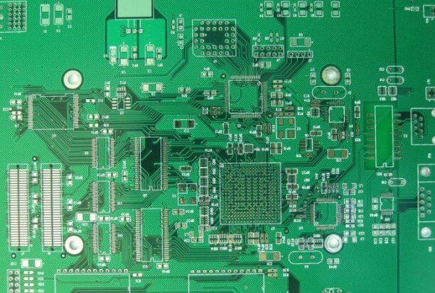
Manufacturing and Application of HDI Boards
HDI board manufacturing is the fastest growing field in the printed circuit board industry. From the first 32-bit computer launched by HP in 1985 to today’s large-scale customer servers using 36 sequentially laminated multi-layer printed circuit boards and stacked micro-vias, HDI/micro-via technology is undoubtedly the future PCB architecture. Large ASICs and FPGAs with smaller device pitches, more I/O pins and embedded passive devices have shorter and shorter rise times and higher frequencies, which all require smaller PCB feature sizes, which has driven a strong demand for HDI/micro-vias.
HDI boards are mainly made using micro-blind buried via technology. The characteristic is that the electronic circuit distribution line density in the printed circuit board is higher. Due to the greatly increased line density, the printed circuit board made of HDI boards cannot be drilled using the general drilling method. HDI must adopt a non-mechanical drilling process. There are quite a few non-mechanical drilling methods, among which “laser drilling” is the main drilling solution for HDI high-density interconnect technology.

1 HDI board process
First-order process: 1+N+1
Second-order process: 2+N+2
Third-order process: 3+N+3
Fourth-order process: 4+N+4
2HDI board source
As electronic products tend to be multifunctional and complex, the distance between the contacts of integrated circuit components is reduced, and the speed of signal transmission is relatively increased. As a result, the number of wiring is increased and the length of the wiring between points is locally shortened. These require the application of high-density circuit configuration and micro-hole technology to achieve the goal. Wiring and jumper are basically difficult to achieve for single- and double-sided boards, so the circuit board will move towards multi-layer. As the signal lines continue to increase, more power layers and ground layers are necessary means of design. These have made multi-layer printed circuit boards (Multilayer Printed Circuit Board) more common.
For the electrical requirements of high-speed signals, the circuit board must provide impedance control with AC characteristics, high-frequency transmission capabilities, and reduce unnecessary radiation (EMI). With the structure of Stripline and Microstrip, multi-layer becomes a necessary design. In order to reduce the quality problem of signal transmission, insulating materials with low dielectric constant and low attenuation rate are used. In order to meet the miniaturization and array of electronic components, the density of circuit boards is constantly increasing to meet the needs. The emergence of component assembly methods such as BGA (Ball Grid Array), CSP (Chip Scale Package), and DCA (Direct Chip Attachment) has pushed printed circuit boards to an unprecedented high density.
Any hole with a diameter less than 150um is called microvia in the industry. The circuit made by using this microvia geometric structure technology can improve the efficiency of assembly, space utilization, etc., and it is also necessary for the miniaturization of electronic products.
For this type of circuit board products, the industry has had many different names to call such circuit boards. For example: European and American companies used to use a sequential construction method in the production process, so they called this type of product SBU (Sequence Build Up Process), which is generally translated as “sequential layering method”. As for Japanese manufacturers, because the hole structure produced by this type of product is much smaller than the previous holes, the production technology of this type of product is called MVP (Micro Via Process), which is generally translated as “micro-hole process”. Some people also call this type of circuit board BUM (Build Up Multilayer Board), which is generally translated as “build-up multilayer board”, because the traditional multilayer board is called MLB (Multilayer Board).
In order to avoid confusion, the IPC Circuit Board Association in the United States proposed to call this type of product a general name HDI (High Density Intrerconnection Technology). If it is directly translated, it becomes high-density connection technology. However, this cannot reflect the characteristics of the circuit board, so most circuit board manufacturers call this type of product HDI board or the full Chinese name “high-density interconnection technology”. However, due to the problem of oral fluency, some people directly call this type of product “high-density circuit board” or HDI board.
3 HDI board application
While electronic design is constantly improving the performance of the whole machine, it is also trying to reduce its size. In small portable products from mobile phones to smart weapons, “small” is an eternal pursuit. High-density integration (HDI) technology can make terminal product design more miniaturized while meeting higher standards of electronic performance and efficiency. HDI is currently widely used in mobile phones, digital (camcorders), MP3, MP4, laptops, automotive electronics and other digital products, among which mobile phones are the most widely used. HDI boards are generally manufactured using the build-up method. The more times the build-up is done, the higher the technical level of the board. Ordinary HDI boards are basically built up once, while high-end HDI boards use two or more build-up technologies, and also use advanced PCB technologies such as stacked holes, electroplated hole filling, and laser direct drilling. High-end HDI boards are mainly used in 3G mobile phones, advanced digital cameras, IC substrates, etc.
Development prospects: According to the use of high-end HDI boards – 3G boards or IC substrates, its future growth is very rapid: the world’s 3G mobile phone growth will exceed 30% in the next few years, and China is about to issue 3G licenses; Prismark, an IC substrate industry consulting agency, predicts that China’s forecast growth rate from 2005 to 2010 will be 80%, which represents the technical development direction of PCBs.
4 Market supply and demand analysis of HDI boards
The continuous growth of mobile phone production drives the growth of demand for HDI boards. China plays an important role in the world’s mobile phone manufacturing industry. Since Motorola fully adopted HDI boards to manufacture mobile phones in 2002, more than 90% of mobile phone motherboards currently use HDI boards. A research report released by market research company In-Stat in 2006 predicted that in the next five years, global mobile phone production will continue to grow at a rate of about 15%, and by 2011, the total sales of global mobile phones will reach 2 billion units.
Domestic HDI board production capacity cannot meet the rapidly growing demand. In recent years, the global HDI mobile phone board production status has undergone major changes: except for the well-known mobile phone board manufacturers ASPOCOM and AT&S, which still supply Nokia with 2-stage HDI mobile phone boards, most of the HDI production capacity of major European and American PCB manufacturers has been transferred from Europe to Asia. Asia, especially China, has become the main supplier of HDI boards in the world. According to Prismark’s statistics, China’s mobile phone production accounted for about 35% of the world’s total in 2006. It is expected that by 2009, China’s mobile phone production will reach 50% of the world’s total, and the purchase amount of HDI mobile phone boards will reach 12.5 billion yuan. From the perspective of major manufacturers, the current production capacity of major domestic manufacturers is less than 2% of the global total demand. Although some manufacturers have invested in expanding production, overall, the growth of domestic HDI production capacity still cannot meet the rapidly growing demand.
5 HDI boards have the following advantages
Can reduce PCB costs: When the density of PCBs increases to more than eight layers, the cost of manufacturing with HDI will be lower than the traditional complex lamination process.
Increase line density: interconnection between traditional circuit boards and parts
Benefits the use of advanced assembly technology
Has better electrical performance and signal accuracy
Better reliability
Can improve thermal properties
Can improve radio frequency interference/electromagnetic interference/electrostatic discharge (RFI/EMI/ESD)
Increase design efficiency
6 HDI board imaging
- While achieving low defect rate and high yield, it can achieve stable production with conventional high-precision operation of HDI. For example:
- Advanced mobile phone board, CSP pitch less than 0.5mm (connection [with or without wire between disks]
- The board structure is 3+n+3, with three stacked vias on each surface,
- 6 to 8 layer coreless PCB with stacked vias
In terms of imaging, such designs require annular widths less than 75 mm, and in some cases even less than 50 mm. These inevitably lead to low yields due to alignment issues. In addition, driven by miniaturization, lines and spacing are getting finer and finer – meeting this challenge requires changing the traditional imaging method. This can be done by reducing the panel size, or by using a shutter exposure machine to image the panel in several steps (four or six). Both methods achieve better alignment by reducing the effects of material deformation. Changing the panel size leads to high material costs, and using a shutter exposure machine leads to low daily yields. Neither method can completely solve the problem of material deformation and reduce defects related to the photographic plate, which includes the actual deformation of the photographic plate when printing batches/lots.
- Achieve the required yield by printing the required number of panels per day. As previously described As mentioned above, the relevant quantity of the required output should be taken into account in the accuracy requirements. To achieve the required output, it is necessary to use automatic control to obtain high output rates.
- Low cost operation. This is the main requirement for any mass production manufacturer. Early LDI modes either required the replacement of the traditional dry film used with a more sensitive dry film to achieve faster imaging speed; or the dry film was replaced with a different band depending on the light source used in the LDI mode. In all these cases, the new dry film is usually more expensive than the traditional dry film used by the manufacturer.
- Compatibility with existing processes and production methods. The processes and methods of mass production are usually carefully specified to meet the requirements of mass production. The introduction of any new imaging method should have minimal changes to the existing methods. This includes minimal changes to the dry film used, the ability to expose various layers of solder mask, traceability functions required by mass production, and more.
KKPCB conducts research on special processing technologies such as ordinary double-sided boards, thick copper circuit boards, high-frequency circuit boards, HDI circuit boards, rigid-flexible circuit boards, FPC flexible boards, buried blind hole circuit boards, and IC carrier boards. Provides PCB design, PCB layout, PCB prototyping and PCB assembly services.


