High-frequency PCB design rules to know
High-frequency PCB design is demanding and requires careful attention to every design detail. This is because the higher the frequency, the more sensitive the signal is to interference and losses. This article brings together high-frequency PCB design guidelines, from the type of materials used to the traces and stack-up or component layout.
What is a high frequency PCB?
A high-frequency PCB is a printed circuit board that can transmit radio waves or RF signals. To understand how it works, we must first understand what a high-frequency circuit is. After that, we will understand the difference between a high-frequency circuit board and other types of PCBs.
High frequency circuit
High-frequency circuits are those that operate within or work in the radio frequency spectrum, which ranges from MHz to GHz . They often require specific components, materials, and manufacturing processes to help them function properly.
These circuits are often used in communication technologies such as satellite systems, mobile phones, Wi-Fi networks, etc. Therefore, high-frequency circuit design requires an understanding of RF design principles and components.
High frequency circuit board
A high-frequency circuit board is a PCB that contains components and materials specifically designed to send and receive radio frequency signals. In addition to these components, a high-frequency circuit board also includes specific types of dielectric and conductor materials.
High-frequency circuits are often affected by the slightest changes in power, inductance, capacitance, and other electrical characteristics. Therefore, it is critical to ensure that your board adheres to specific design rules.
High frequency PCB design
High-frequency PCB design includes everything you need to create a PCB that can transmit RF signals accurately and efficiently. This is usually possible – and necessary – when designing a circuit board.
For example, board stackup, component placement, and materials must be carefully considered to ensure proper signal transmission. Other considerations include trace width, which will depend on the signal frequency used, and impedance control , which is important for RF signals.
Just as when designing other types of boards, high-frequency PCB design is made possible by incorporating tools found in board software. This software allows for the correct placement of components, setting up impedance-controlled circuits, and routing traces—all necessary to ensure that the board functions properly.

High Frequency PCB Design Rules
In the design of high-frequency PCBs, specific design rules apply. For example, these rules can help designers eliminate crosstalk, or allow them to introduce impedance control. To ensure that your board design meets high-frequency standards, consider the following:
High frequency PCB materials
High-frequency circuit boards require specific materials designed to transmit radio signals efficiently. These include special substrates, laminates, and copper foil, as well as any other materials used in the circuit board’s construction.
Each of these high-frequency PCB materials should be carefully selected to ensure that it can handle high-frequency signals without interference or signal loss. In particular, the substrate or laminate should be designed for RF, otherwise problems such as signal attenuation will occur.
FR-4 is generally not recommended due to its higher dielectric losses at higher frequencies. Instead, other materials such as Rogers 4350B, Isola, and Tachyon are preferred. These excel in high-frequency applications.
High Frequency PCB Stackup
Stackup is an important factor in high-frequency circuit design. The number of layers and their arrangement will directly affect the performance of the signal. A standard high-frequency PCB stackup will include a power layer, multiple ground layers, and a signal layer between these power and ground layers.
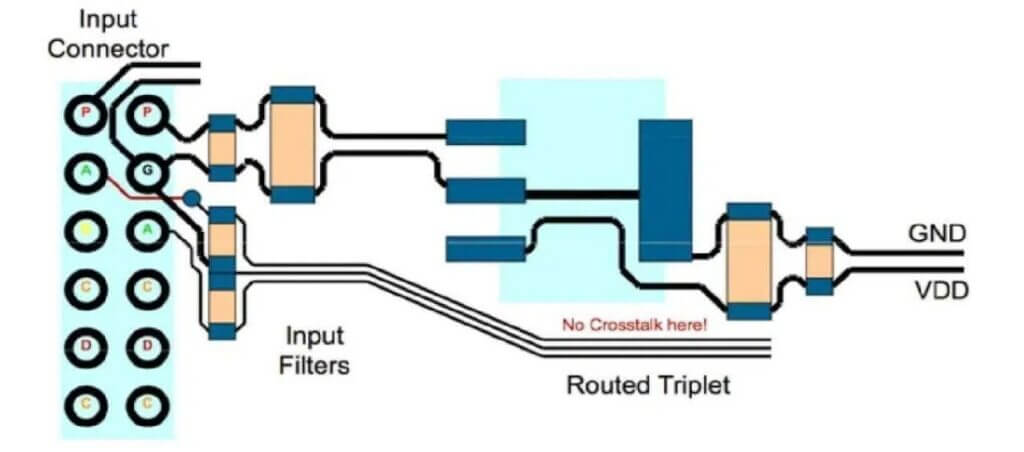
To avoid crosstalk in such stackups, always use ground planes to isolate signal layers. Also, increase the distance between signal layers to minimize crosstalk.
Other high-frequency PCB design rules for stackup include the use of adjacent layers or vertical orientation, and the use of microvias to reduce inductance and improve signal integrity. Digital signals should also be separated from analog signals for better performance.
Wiring high frequency PCB
The key to successful high-frequency PCB layout is to ensure that signal loss is minimized. To do this, designers must pay close attention to routing and component placement.
To avoid coupling interference, consider using orthogonal routing to keep signal noise low. Microstrip and stripline routing techniques can also be used to reduce signal loss.
A fly-by topology for long signal traces, with as much separation as possible between each stack-up layer, will help reduce reflections and other signal losses.
Pay attention to the lead length between pins of high-frequency circuits. Shorter leads reduce signal loss. If longer leads are required, make sure they are a consistent length between pins for best performance.
High frequency PCB impedance control
When designing a high frequency board, it is critical to keep impedance under control. To ensure this, several design rules must be followed. First, make sure you use the correct trace width for the desired impedance. Shorter traces help reduce inductance, while wider traces help increase impedance .
Use the 3 or 2W rule to separate traces and control their impedance. This rule states that for best impedance control, the spacing between traces should be at least 3 or XNUMX times their width.
As mentioned previously, using a ground plane can reduce crosstalk and signal loss. Placing the ground line directly underneath the signal line will help achieve better impedance control.
Pay attention to the transition of layers when routing high-frequency circuit signals. Ensure the transition from one layer to another is as smooth as possible, and use microvias to avoid signal reflections.
in conclusion
High-frequency PCB design requires special considerations to ensure optimal performance of the board. These include rules that consider material selection, stackup, routing, and impedance control. By following these guidelines and taking the necessary steps, designers can create a high-frequency board that produces reliable results.


