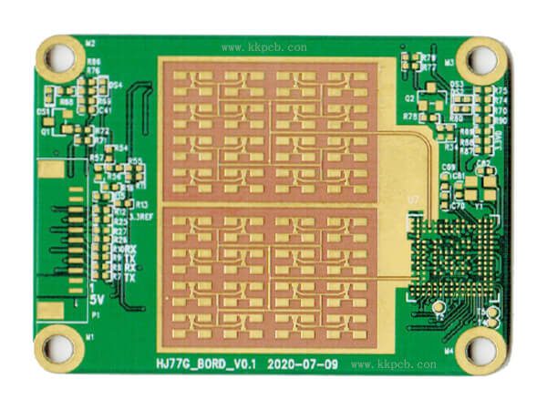
High-frequency PCB design High frequency signal PCB wiring skills
In today’s fast-developing electronic age, PCB printed circuit boards are the heart of electronic products, and their design and manufacturing technologies are constantly improving, especially in the field of high-frequency circuits. High-frequency PCB design is not only related to the performance stability of the product, but also directly affects signal integrity and electromagnetic compatibility (EMC). This article will unveil the mystery of high-frequency signal PCB wiring for you, and take you to a deep understanding of the key elements and design techniques in this field.
1. Basics of high-frequency PCB design
High-frequency PCB usually refer to circuit systems with operating frequencies above 100MHz. In this frequency range, many assumptions of traditional low-frequency circuit design are no longer applicable, and challenges such as transmission line effects, signal integrity issues, and electromagnetic interference (EMI) begin to emerge. Therefore, high-frequency PCB design requires a series of special design principles and strategies to ensure signal quality and system reliability.
2. Transmission Line Theory and Matching
In high-frequency circuits, signal lines are regarded as transmission lines, and the continuity and matching of their characteristic impedance become critical. Improper impedance matching can lead to signal reflection, affecting signal integrity and the stable operation of the system. Common impedance control methods include selecting appropriate line width, line spacing, dielectric thickness, and using a specific stacking structure to achieve an ideal characteristic impedance value (commonly 50Ω or 75Ω).

3. High-frequency signal wiring skills
Short and straight : High-frequency signal lines should be as short and straight as possible, with fewer corners, to reduce the inductance of the signal path and reduce transmission delay.
Number of layers and stacking : Multilayer PCB board design helps isolate different signals and reduce cross-interference. High-frequency PCB signals are usually arranged on the inner layer and as close to the ground plane as possible, using the ground plane as a return path to enhance the shielding effect of the signal.
Impedance control and matching : Use advanced PCB design software for simulation analysis to ensure that the characteristic impedance of all transmission lines is consistent, and implement impedance matching at the signal source and load ends.
Decoupling and bypassing : The purity of the power supply and ground plane in High-frequency PCB has a great impact on signal quality. Reasonable layout of decoupling capacitors, especially high-frequency ceramic capacitors, can effectively filter out power supply noise and maintain voltage stability.
Differential pair wiring : For high-speed differential signals, keeping the two lines of equal length and consistent spacing helps improve the signal’s anti-interference ability and is the preferred solution for high-frequency signal transmission.
4. Electromagnetic compatibility considerations
high-frequency PCB design must strictly control EMI/EMC issues. This includes adopting appropriate shielding measures, designing a good grounding system, arranging the location of high-frequency components, and applying filtering technology. In addition, conducting EMC testing to ensure that the product meets relevant electromagnetic compatibility standards is an indispensable part of the product development process.
high-frequency PCB design is a complex and delicate task, requiring designers to have profound theoretical knowledge and rich practical experience. Through precise impedance control, optimized wiring strategy, and strict EMC management, the performance and reliability of high-frequency circuits can be effectively improved. With the continuous advancement of technology, the emergence of new materials, processes, and design tools will continue to promote the development of high-frequency PCB design and provide more possibilities for the innovation of future electronic products.
KKPCB provides global customers with one-stop services from PCB layout, prototype PCB proofing, PCB manufacturing, PCBA processing (including SMT and DIP), PCBA testing, PCBA product assembly and outbound packaging. You could provide a Gerber file or BOM list to us, we will offer the finished PCB products or PCB assembly which are satisfied with you.


