8 Best Tips and Key Considerations for Designing High-Voltage PCBs
Designing a high-voltage PCBs requires careful planning, adherence to specific guidelines, and a keen eye for safety. Whether you’re working on industrial equipment, power electronics, or consumer devices, the following tips and considerations will ensure you create efficient and safe high-voltage PCB designs.
1. Routing Guidelines for High-Voltage PCBs
Proper routing is crucial for high-voltage PCB reliability. Keep these points in mind:
- Clearance Between Traces: Maintain adequate spacing between traces carrying large voltage differences to prevent arcing.
- Avoid Sharp Edges: Use smooth curves instead of sharp corners to minimize high electric field concentrations.
- Layer Placement: Avoid placing high-voltage lines on inner PCB layers to prevent insulation breakdown.
2. Optimizing Polygon Planes
In high-voltage PCB designs:
- Increase polygon plane clearance around high-voltage traces.
- Ensure proper separation between inner layers to reduce the risk of short circuits.
Tip: A safe polygon plane design prevents current leakage and ensures operational stability.
3. Layer Management in Multilayer PCBs
When designing multilayer PCBs:
- Use medium voltage layers and maintain at least a 0.005-inch gap between layers to maintain dielectric integrity.
- Avoid using traditional FR4 prepreg for medium and high-voltage designs, as it has limited dielectric uniformity and can degrade quickly.
Material Upgrade Suggestion: Opt for materials like BT epoxy or polyimide for enhanced dielectric strength.
4. Electromagnetic Interference (EMI) Considerations
High-voltage circuits can generate significant EMI. To mitigate this:
- Minimize loop areas in your PCB layout.
- Use ground plane stitching and, where necessary, add metal shields for isolation.
5. High-Frequency Transformers and Isolation
When designing for transformer-based circuits:
- Adhere to the insulation requirements for transformer cores.
- Separate the primary and secondary sides with clear isolation gaps and cutouts on the PCB.
Pro Tip: Splitting the ground plane between transformer sides improves isolation and safety.
6. Passive Components and Packaging
Choosing the right components is essential:
- For high voltages, use components with higher package sizes (e.g., 1206 instead of 0402).
- When needed, connect multiple components in series to distribute voltage stress.
7. Isolation Cutouts and Slots
To prevent electrical hazards:
- Add isolation cutouts or slots near high-voltage components.
- These features help meet safety standards, especially in high-humidity or contamination-prone environments.
8. Material Selection for High-Voltage PCBs
Selecting the right PCB material is critical for withstanding high voltage:
- BT Epoxy and polyimide are excellent for high-voltage applications.
- Avoid using standard FR4, as it lacks sufficient dielectric strength.
Surface Finish: Ensure a flat and even finish to avoid sharp points or imperfections, which can create strong electric fields and cause arcing.
Creepage and Clearance in High-Voltage PCB Design
Proper spacing is essential to avoid arcing and ensure safety. Two key distances to consider are:
Electrical Clearance
- The shortest air gap between two conductors with a potential difference.
- Factors like humidity and dust can reduce clearance effectiveness, increasing the risk of arcing.
Creepage Distance
- The shortest distance along the insulating surface between two conductors.
- Use techniques like adding isolation slots or vertical barriers to meet creepage distance requirements.
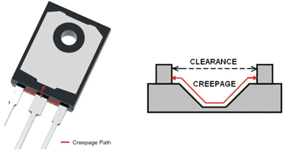
Reference Standards: Follow IPC-2221 and IEC-60950-1 guidelines for clearance and creepage distances in high-voltage PCBs.
FAQ: High-Voltage PCB Design
What constitutes high voltage for PCBs?
Typically, PCBs operating at 100V or higher are considered high voltage.
What is the maximum voltage a PCB can withstand?
Low-cost PCB materials can handle up to 1000 volts. For higher voltages, specialized materials are required.
How much current can a PCB via carry?
A 0.35 mm via can carry up to 2 amps safely. Filling vias with solder reduces resistance.
How hot can PCB traces get?
PCB traces typically operate within 20–30°C above ambient temperature. Internal temperatures exceeding 105°C may lead to material degradation and UL certification issues.
Designing high-voltage PCBs involves balancing electrical, mechanical, and material considerations. By following these guidelines and using reliable materials and manufacturers, you can ensure your high-voltage PCB is safe, durable, and efficient. Remember, precision in design and adherence to industry standards is the key to success.


